

 English
FGM842D TE-B User Guide
Introduction
This document introduces the FGM842D series TE-B and its hardware and air interface connections with customer applications. It helps customers quickly understand the hardware interface characteristics, RF characteristics, electrical characteristics, mechanical specifications, and other related information of the FGM842D series TE-B.
Product Overview
The FGM842D series TE-B is a development board that supports all interfaces of the FGM842D series. It can be used for basic functionality testing and further development of the FGM842D series.
Top View and Bottom View
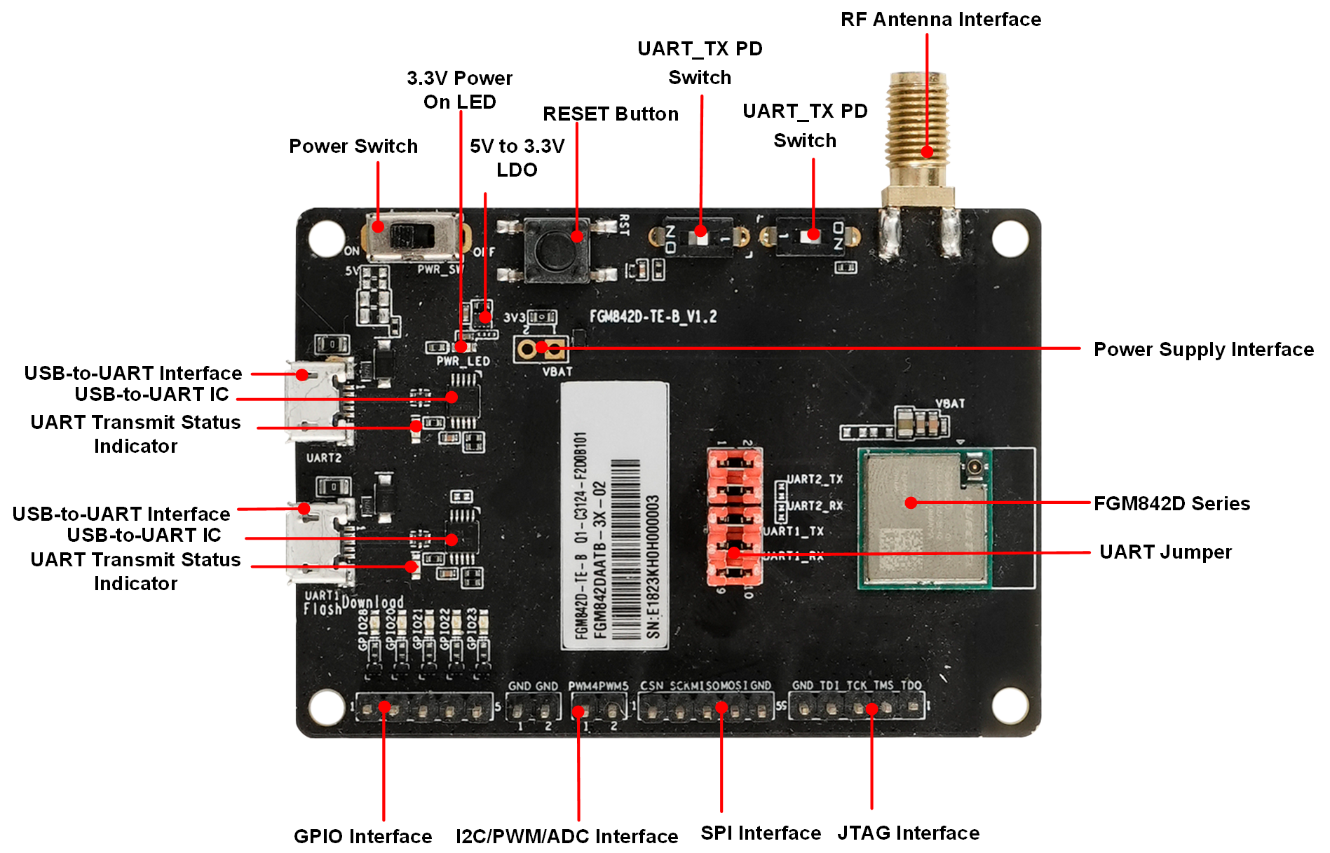
TE-B Component Layout
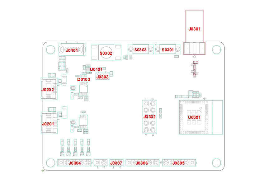
| Component Name | Reference Designator | Description |
|---|---|---|
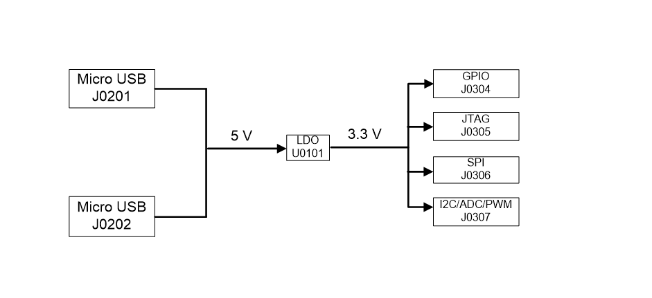
| Power Interface | J0201, J0202 | USB power supply interface |
| J0303 | External 3.3 V power interface | |
| LDO | U0101 | 5 V to 3.3 V |
| FGM842D Series | U0301 | FGM842D series module |
| Power Switch | J0101 | VBAT on/off control |
| USB-to-UART Interface | J0201 | UART1 interface (main UART) |
| J0202 | UART2 interface (debug UART) | |
| RF Antenna Interface | J0301 | RF SMA connector |
| UART Switch | J0302 | UART1/UART2 jumper cap control |
| Reset Button | S0302 | Reset module for firmware upgrade |
| Power Indicator | D0103 | Indicates power on/off status |
| UART_TX Pull-down Switch | S0301, S0303 | Module enters RF test mode |
| GPIO Interface | J0304 | Tests GPIO functionality of the module |
| JTAG Interface | J0305 | Tests JTAG functionality of the module |
| SPI Interface | J0306 | Tests SPI functionality of the module |
| I2C/PWM/ADC Interface | J0307 | Tests I2C/PWM/ADC functionality of the module |
Key Features
| Parameter | Description |
|---|---|
| Power Supply | USB Power Supply: 4.75 ~ 5.25 V Typical: 5 V External Power Supply: 3.0 ~ 3.6 V Typical: 3.3 V |
| Temperature Range | Operating Temperature: -40 °C ~ +105 °C 1 Storage Temperature: -45 °C ~ +115 °C |
| UART Switch | UART1/UART2 jumper cap control |
| USB-to-UART Interface | Provides 2 UARTs UART1: Used for firmware upgrade and AT command communication, supports baud rate of 115200 bps (default) UART2: Used for debugging and log output, supports baud rate of 921600 bps (default) |
| Reset Button | Resets the module for firmware upgrade |
| Dimensions | (70 ±0.15) mm × (50 ±0.15) mm × (1.6 ±0.2) mm |
| Firmware Upgrade | Via UART1 or FOTA |
| Antenna Interface | 50 Ω characteristic impedance |
Functional Block Diagram
Operating Instructions
The FGM842D series TE-B is used for firmware upgrades or development and debugging of IoT applications based on the FGM842D series modules. The following sections introduce the specific operation process:
Getting Started
Interface Diagram
Operating Steps
Download and install the USB-to-UART chip driver. The driver can be downloaded from the following link: CH341SER.EXE;
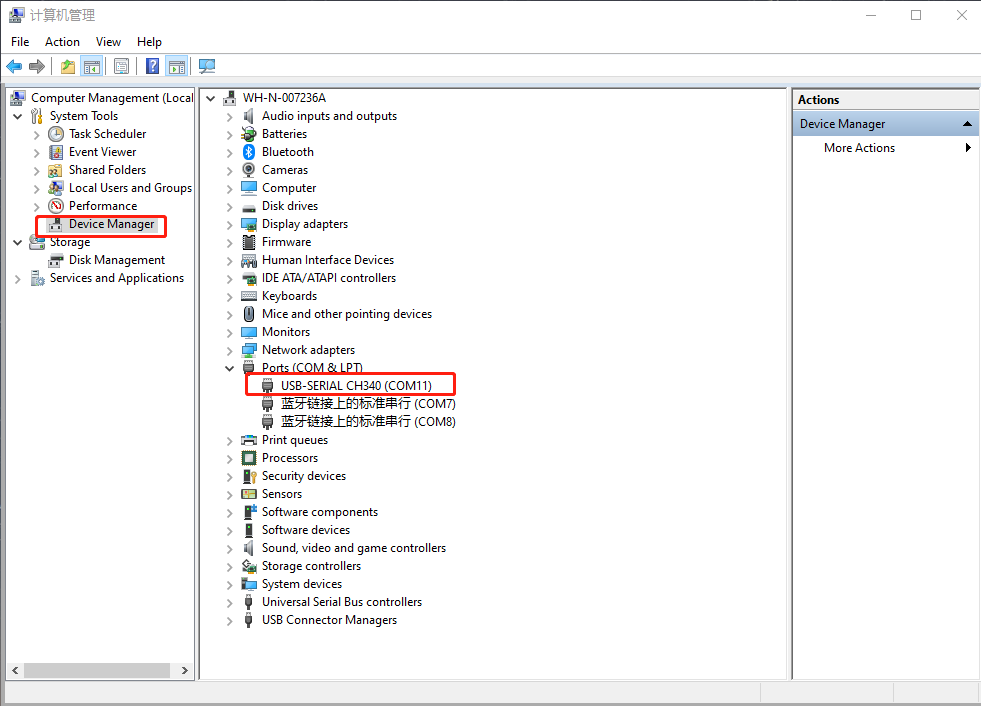
Use a Micro USB data cable to connect J0201 or J0202 (USB-to-UART interface) to the computer. Then, check the "Device Manager" on the computer to see the serial port as shown below. "USB-SERIAL CH340 (COM11)" connects to the TE-B's UART1 (main UART) for firmware upgrades and AT command communication. If connected to the TE-B's UART2 (debug UART), it is used for debugging and log output. For more details on UART configuration, refer to Harware Design.
During use, S0302 can be used to reset the module.
Power Consumption Testing Guide
For more detailed power consumption test steps and instructions, please refer to Power Consumption Test.
Testing Tools
Tools and equipment required for power consumption testing:
- FGM842D series TE-B;
- DC power analyzer;
- Wires, soldering iron, solder, and wire stripper for soldering power supply wires on the TE-B.
Power Consumption Testing
To test power consumption in maximum transmission power, sleep, and other states using the TE-B, follow these steps:
Remove the resistor at reference designator R0307 to disconnect the module from other parts;
Solder a wire to pin 1 of J0303 as the VBAT power supply terminal for the module; solder a wire to any pin of J0201 as GND. This allows the external power supply to independently power the module;
Use a DC power analyzer to supply 3.3 V to the soldered wires. The module will power on automatically;
Connect the TE-B to a PC using a Micro USB data cable and perform power consumption testing in different modes.
Appendix Reference Documents
| Term | English Description |
|---|---|
| ADC | Analog-to-Digital Converter |
| FOTA | Firmware Over-The-Air |
| LDO | Low-dropout Regulator |
| GPIO | General-Purpose Input/Output |
| PWM | Pulse Width Modulation |
| SMA | Sub Miniature Version A |
| SPI | Serial Peripheral Interface |
| UART | Universal Asynchronous Receiver & Transmitter |
| USB | Universal Serial Bus |
Indicates that when the product operates within this temperature range, its performance complies with IEEE 802.11 and Bluetooth SIG standards.↩