

 English
HCM111Z Hardware Design
Introduction
QuecOpen® is a solution where the module acts as the main processor.Constant transition and evolution of both the communication technology and the market highlight its merits. It can help you to:
- Realize embedded applications' quick development and shorten product R&D cycle
- Simplify circuit and hardware structure design to reduce engineering costs
- Miniaturize products
- Reduce product power consumption
- Apply OTA technology
- Enhance product competitiveness and price-performance ratio
This document defines HCM111Z in QuecOpen® solution and describes its hardware interfaces and air interfaces, which are connected with your applications. The document provides a quick insight into interface specifications, RF performance, electrical and mechanical specifications, as well as other related information of the module.
Special Marks
Special Marks:
| Mark | Definition |
|---|---|
| * | Unless otherwise specified, an asterisk () after a function, feature, interface, pin name, command, argument, and so on, indicates that it is under development and currently not supported; and the asterisk () after a model indicates that the model sample is currently unavailable. |
| [...] | Brackets ([…]) used after a pin enclosing a range of numbers indicate all pins of the same type. For example, SDIO_DATA[0:3] refers to all four SDIO pins: SDIO_DATA0, SDIO_DATA1, SDIO_DATA2, and SDIO_DATA3. |
Product Overview
HCM111Z is a low-power and high performance MCU Bluetooth module compliant with BLE 5.3 protocol. The module supports multiple interfaces such as UART, SWD, I2C, ADC, PWM and SPI for various applications.
It is an SMD module with compact packaging. The general features of the module are as follows:
- Embedded 32-bit ARM Cortex-M3 processor with a frequency of up to 48MHz
- 48 KB SRAM memory and 512 KB Flash
- Supporting OTA (Over-The-Air Upgrade)
- Supporting secondary development
Basic Information:
| HCM111Z | |
|---|---|
| Packaging type | LCC |
| Pin counts | 23 |
| Dimensions | (15 ±0.2) mm × (12 ±0.2) mm × (2.25 ±0.2) mm |
| Weight | Approx. 0.62 g |
Key Features
Key Features:
| Basic Information | |
|---|---|
| Protocols and Standards | |
| Power Supply | VBAT Power Supply: |
| Temperature Ranges | |
| TE-B Kit | HCM111Z-TE-B 2 |
| Antenna/Antenna Interface | |
| Antenna/Antenna Interface 3 | |
| Application Interfaces 4 | |
| Application Interfaces | UART, SWD, I2C, ADC, PWM, SPI, LED, analog audio interfaces* (optional) |
Functional Diagram
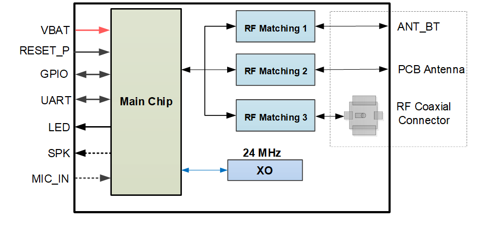
NOTE:
- The module is provided with one of the three antenna/antenna interface designs. For more details, contact Quectel Technical Support.
- The analog audio interfaces* are optional. If unused, keep them open. For more details, contact Quectel Technical Support.
Application Interfaces
Pin Assignment
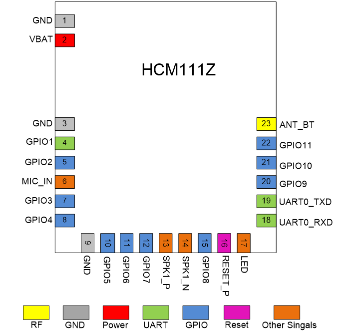
NOTE:
- Keep all RESERVED and unused pins unconnected.
- All GND pins should be connected to ground.
- The module provides 10 GPIO interfaces by default. In the case of multiplexing, it supports interfaces including UART, SWD, I2C, ADC, PWM and SPI. For more details, see Chapter 3.3 andChapter 3.4.
Pin Definitions
Parameter Description:
| Parameter | Description |
|---|---|
| AI | Analog Input |
| AO | Analog Output |
| AIO | Analog Input/Output |
| DI | Digital Input |
| DO | Digital Output |
| DIO | Digital Input/Output |
| PI | Power Input |
DC characteristics include power domain and rated current.
Pin Description:
Power Supply and GND Pins:
| Pin Name | Pin No. | I/O | Description | DC Characteristics | Comment |
|---|---|---|---|---|---|
| VBAT | 2 | PI | Power supply for the module | Vmin = 2.4 V Vnom = 3.3 V Vmax = 4.3 V |
It is recommended to provide with sufficient current of 100 mA at least. |
| GND | 1, 3, 9 |
Reset:
| Pin Name | Pin No. | I/O | Description | DC Characteristics | Comment |
|---|---|---|---|---|---|
| RESET_P | 16 | DI | Reset the module | VIO 5 | Active high. |
UARTs:
| Pin Name | Pin No. | I/O | Description | DC Characteristics | Comment |
|---|---|---|---|---|---|
| UART0_TXD | 19 | DO | UART0 transmit | VIO | |
| UART0_RXD | 18 | DI | UART0 receive | VIO | |
| GPIO1 | 4 | DO | UART1 transmit | VIO | Only used as debugging for standard firmware. |
GPIO Interfaces:
| Pin Name | Pin No. | I/O | Description | DC Characteristics | Comment |
|---|---|---|---|---|---|
| GPIO2 | 5 | DIO | General-purpose input/output | VIO | |
| GPIO3 | 7 | DIO | General-purpose input/output | VIO | |
| GPIO4 | 8 | DIO | General-purpose input/output | VIO | |
| GPIO5 6 | 10 | DI | Sleep wake-up control | VIO | It can be configured as either “sleep wake-up control” or “general-purpose input/output” function through APIs in QuecOpen® solution. |
| GPIO5 | 10 | DIO | General-purpose input/output | VIO | It can be configured as either “sleep wake-up control” or “general-purpose input/output” function through APIs in QuecOpen® solution. |
| GPIO6 | 11 | DIO | General-purpose input/output | VIO | |
| GPIO7 | 12 | DIO | General-purpose input/output | VIO | |
| GPIO8 | 15 | DIO | General-purpose input/output | VIO | |
| GPIO9 | 20 | DIO | General-purpose input/output | VIO | |
| GPIO10 | 21 | DIO | General-purpose input/output | VIO | |
| GPIO11 7 | 22 | DO | Message notification indication | VIO | It can be configured as either “message notification indication” or “general-purpose input/output” function through APIs in QuecOpen® solution. |
| GPIO11 | 22 | DIO | General-purpose input/output | VIO | It can be configured as either “message notification indication” or “general-purpose input/output” function through APIs in QuecOpen® solution. |
Analog Audio Interfaces* (Optional): 8
| Pin Name | Pin No. | I/O | Description | DC Characteristics | Comment |
|---|---|---|---|---|---|
| MIC_IN | 6 | AI | Microphone input | If unused, keep them open. | |
| SPK1_P | 13 | AO | Analog audio differential output 1 (+) | If unused, keep them open. | |
| SPK1_N | 14 | AO | Analog audio differential output 1 (-) | If unused, keep them open. |
LED Interface:
| Pin Name | Pin No. | I/O | Description | DC Characteristics | Comment |
|---|---|---|---|---|---|
| LED | 17 | DO | LED output control | VIO | If unused, keep it open. |
RF Antenna Interface:
| Pin Name | Pin No. | I/O | Description | DC Characteristics | Comment |
|---|---|---|---|---|---|
| ANT_BT | 23 | AIO | Bluetooth antenna interface | 50 Ω characteristic impedance. |
GPIO Multiplexing
The module provides 10 GPIO interfaces by default, and can support up to 13 GPIO interfaces in the case of multiplexing. Pins are defined as follows:
| Pin Name | Pin No. | Multiplexing Function 0 (GPIO No.) | Multiplexing Function 1 | Multiplexing Function 2 | Multiplexing Function 3 | Multiplexing Function 4 | Multiplexing Function 5 | Multiplexing Function 6 | Multiplexing Function 7 |
|---|---|---|---|---|---|---|---|---|---|
| GPIO1 | 4 | PC7 | I2C1_SDA | PWM5 | UART0_TXD | - | - | SWDIO | SPI_MISO |
| GPIO2 | 5 | PC6 | I2C1_SCL | PWM4 | UART0_RXD | UART1_RXD | - | SWCLK | SPI_MOSI |
| GPIO3 | 7 | PA6 | I2C1_SCL | PWM0 | UART0_RXD | UART1_RXD | - | CLK_OUT | SPI_ MOSI |
| GPIO4 | 8 | PA7 | I2C1_SDA | PWM1 | UART0_TXD | UART1_TXD | - | ANT_CTL0 | SPI_MISO |
| GPIO5 | 10 | PA1 | I2C0_SDA | PWM1 | UART0_TXD | UART1_TXD | - | ANT_CTL0 | SPI_CS |
| GPIO6 | 11 | PC5 | I2C0_SDA | PWM5 | UART0_TXD | UART1_TXD | - | - | SPI_CS |
| GPIO7 | 12 | PA0 | I2C0_SCL | PWM0 | UART0_RXD | UART1_RXD | - | CLK_OUT | SPI_CLK |
| GPIO8 | 15 | PD4 | I2C0_SCL | PWM4 | UART0_RXD | UART1_RXD | ADC0 | ANT_CTL0 | SPI_CLK |
| GPIO9 | 20 | PD6 | I2C1_SCL | PWM0 | UART0_RXD | UART1_RXD | ADC2 | CLK_OUT | SPI_ MOSI |
| GPIO10 | 21 | PD5 | I2C0_SDA | PWM5 | UART0_TXD | UART1_TXD | ADC1 | ANT_CTL0 | SPI_CS |
| GPIO11 | 22 | PD7 | I2C1_SDA | PWM1 | UART0_TXD | UART1_TXD | ADC3 | ANT_CTL1 | SPI_MISO |
UART0_ TXD |
19 | PA3 | I2C1_SDA | PWM3 | - | UART1_TXD | - | ANT_CTL1 | - |
UART0_ RXD |
18 | PA2 | I2C1_SCL | PWM2 | - | UART1_RXD | - | ANT_CTL0 | - |
NOTE:
- The maximum number of each application interface multiplexed through GPIOs isn't available simultaneously. For the maximum number of different application interfaces that the module can support, see Chapter 3.4 for details.
- After the module is powered off, all of its GPlOs must be driven low. Otherwise, the current leakage may make the module enter an abnormal state.
Application Interfaces
UARTs
The module supports 1 UART0 by default, and GPIO1 is only used for debugging of standard firmware. In the case of multiplexing, it can
support up to 2 UARTs: UART0 and UART1. See Table 6 for more details. The pin definition of default UARTs is as follows:
Pin Definition of UARTs:
| Pin Name | Pin No. | I/O | Description | Comment |
|---|---|---|---|---|
| UART0_TXD | 19 | DO | UART0 transmit | |
| UART0_RXD | 18 | DI | UART0 receive | |
| GPIO1 | 4 | DO | UART1 transmit | Only used for debugging of standard firmware. |
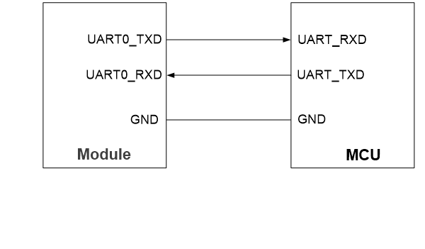
UART0 can be used for AT command communication, data transmission, and firmware upgrade. The baud rate can be configured by yourself. The
default baud rate is 115200 bps. Among them, only the module's default UART0 (pins 18 and 19) can be used for firmware upgrade.
The UART0 connection between the module and MCU is illustrated below.
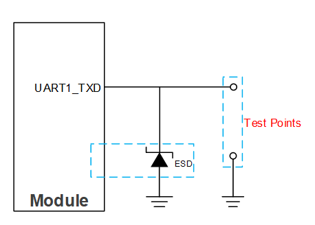
UART1 can be used as debug UART with debugging tools and supports 921600bps baud rate by default. The debugging of standard firmware uses GPIO1(pin 4) only. The following is a reference design for debug UART.

SWD Interface
The module supports 1 SWD interface multiplexed from GPIOs. The SWDvinterface supports online programming.
Pin Definition of SWD Interface:
| Pin Name | Pin No. | Multiplexing Function | I/O | Description |
|---|---|---|---|---|
| GPIO1 | 4 | SWDIO | DIO | Serial data input/output |
| GPIO2 | 5 | SWCLK | DI | Serial clock input |
The common connection of SWD interface is shown below.
I2C Interfaces
In the case of multiplexing, the module supports up to 2 I2C interfaces supporting master and slave modes, and the main features are as follows:
- AMBA 2.0 APB bus protocol
- Programmable master-slave mode
- 7-bit and 10-bit addressing modes
- Automatic clock stretching
- Programmable clock and data timing
- Support for interrupt mode
Pin Definition of I2C Interfaces:
| Pin Name | Pin No. | Multiplexing Function | I/O | Description | Comment |
|---|---|---|---|---|---|
| GPIO3 | 7 | I2C1_SCL | OD | I2C1 serial clock | Other configurations for I2C, see Table 6. |
| GPIO4 | 8 | I2C1_SDA | OD | I2C1 serial data | Other configurations for I2C, see Table 6. |
| GPIO5 | 10 | I2C0_SDA | OD | I2C0 serial data | Other configurations for I2C, see Table 6. |
| GPIO7 | 12 | I2C0_SCL | OD | I2C0 serial clock | Other configurations for I2C, see Table 6. |
ADC Interfaces
In the case of multiplexing, the module supports up to 4 ADC interfaces.To improve ADC accuracy, surround ADC trace with ground.
Pin Definition of ADC Interfaces:
| Pin Name | Pin No. | Multiplexing Function | I/O | Description |
|---|---|---|---|---|
| GPIO8 | 15 | ADC0 | AI | General-purpose ADC interface |
| GPIO9 | 20 | ADC2 | AI | General-purpose ADC interface |
| GPIO10 | 21 | ADC1 | AI | General-purpose ADC interface |
| GPIO11 | 22 | ADC3 | AI | General-purpose ADC interface |
ADC Features:
| Parameter | Min. | Typ. | Max. | Unit |
|---|---|---|---|---|
| ADC Input Voltage Range | 0 | 2.9 | 3.3 | V |
| ADC Resolution Rate | - | 10 | - | bit |
PWM Interfaces
In the case of multiplexing, the module supports up to 6 PWM interfaces,and the pin definitions are shown in the table below.
Pin Definition of PWM Interfaces:
| Pin Name | Pin No. | Multiplexing Function | I/O | Description | Comment |
|---|---|---|---|---|---|
| GPIO9 | 20 | PWM0 | DO | PWM0 output | Other configurations for PWM, seeTable 6. |
| GPIO11 | 22 | PWM1 | DO | PWM1 output | Other configurations for PWM, seeTable 6. |
| UART0_RXD | 18 | PWM2 | DO | PWM2 output | Other configurations for PWM, seeTable 6. |
| UART0_TXD | 19 | PWM3 | DO | PWM3 output | Other configurations for PWM, seeTable 6. |
| GPIO8 | 15 | PWM4 | DO | PWM4 output | Other configurations for PWM, seeTable 6. |
| GPIO10 | 21 | PWM5 | DO | PWM5 output | Other configurations for PWM, seeTable 6. |
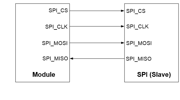
SPI
The module provides 1 SPI multiplexed with GPIOs supporting master mode with a maximum clock frequency of up to 24 MHz.
Pin Definition of SPI:
| Pin Name | Pin No. | Multiplexing Function | I/O | Description | Comment |
|---|---|---|---|---|---|
| GPIO3 | 7 | SPI_MOSI | DO | SPI master-out slave-in | Other multiplexed SPI configurations are shown inTable 6. |
| GPIO4 | 8 | SPI_MISO | DI | SPI master-in slave-out | Other multiplexed SPI configurations are shown inTable 6. |
| GPIO6 | 11 | SPI_CS | DO | SPI chip select | Other multiplexed SPI configurations are shown inTable 6. |
| GPIO7 | 12 | SPI_CLK | DO | SPI clock | Other multiplexed SPI configurations are shown inTable 6. |
The SPI connection is shown below.
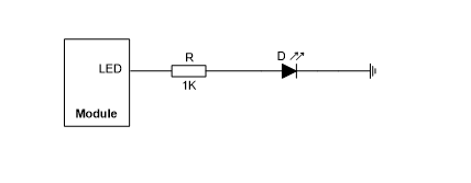
LED Interface
The module provides an LED interface to control LED output.
Pin Definition of LED Interface:
| Pin Name | Pin No. | I/O | Description | Comment |
|---|---|---|---|---|
| LED | 17 | DO | LED output control | If unused, keep it open. |
It is recommended to drive it directly. A reference circuit is shown in the following figure.
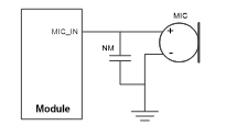
Analog Audio Interfaces* (Optional) 9
The module provides two analog audio interfaces: one for input of microphone and another for analog audio output.
Pin Definition of Audio Interfaces:
| Pin Name | Pin No. | I/O | Description | Comment |
|---|---|---|---|---|
| MIC_IN | 6 | AI | Microphone input | If unused, keep them open. |
| SPK1_P | 13 | AO | Analog audio differential output 1 (+) | If unused, keep them open. |
| SPK1_N | 14 | AO | Analog audio differential output 1 (-) | If unused, keep them open. |
The microphone input reference design is shown in the following figure.
The analog audio output reference design is shown in the following figure.
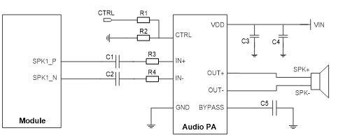
To drive the speaker, an additional power amplifier is needed because the voice output signal from the module is weak. The HT6872, LM4871,CS5620E, and other models are examples of power amplifiers. Depending on the power amplifier model, different peripheral circuit designs exist.For further information, see the appropriate model product design specification.
Operating Characteristics
Power Supply
Power supply pin and ground pins of the module are defined in the following table.
Pin Definition of Power Supply and GND Pins:
| Pin Name | Pin No. | I/O | Description | Min. | Typ. | Max. | Unit |
|---|---|---|---|---|---|---|---|
| VBAT | 2 | PI | Power supply for the module | 2.4 | 3.3 | 4.3 | V |
| GND | 1, 3, 9 |
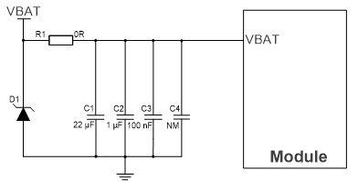
Reference Design for Power Supply
The module is powered by VBAT, and it is recommended to use a power supply chip that provides at least 100 mA to ensure sufficient current.For better power supply performance, it is recommended to parallel a 22μF decoupling capacitor, and two filter capacitors (1 μF and 100 nF)near the module's VBAT pin. C4 is reserved for debugging and not mounted by default. In addition, it is recommended to add a TVS near the VBAT to improve the surge voltage bearing capacity of the module. In principle,the longer the VBAT trace is, the wider it should be.
VBAT reference circuit is shown below:
Turn-on
The module can automatically start up after the VBAT is powered on. The turn-on timing is shown below:
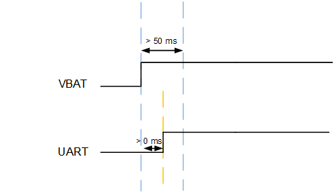
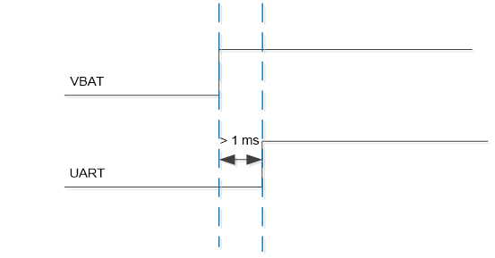
Please make sure that the module VBAT is powered on at least 1 ms before the UART in order to guarantee the module's proper startup and prevent UART voltage backflow.
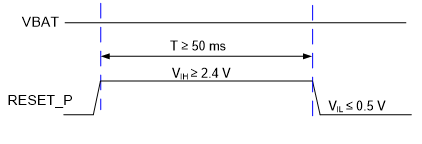
RESET_P
Pull RESET_P up for at least 50 ms and then release it to reset the module.
Pin Definition of RESET_P:
| Pin Name | Pin No. | I/O | Description | Comment |
|---|---|---|---|---|
| RESET_P | 16 | DI | Reset the module | Active high. |
The reference design for resetting the module is shown below. Connect an external power supply (the voltage range is 2.4--3.3 V and the absolute maximum rating is 3.6 V) and RESET_P pin through a button. Press the button to pull up RESET_P, thereby resetting the module. And the button needs to be connected to a large capacitor (about 10 μF) in parallel. At the same time, it is recommended to place a TVS near the button for ESD protection.
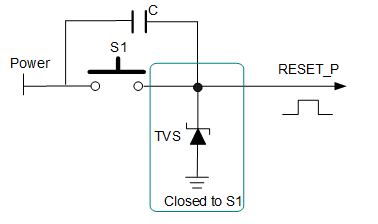
The module reset timing is illustrated in the following figure.
Download Mode
During the module reset or power-on, when the host computer starts the download tool, the module will enter download mode. In the download mode, the firmware can be downloaded through the default UART0 (pins 18 and 19).
RF Performances
Bluetooth Performances
Bluetooth Performances:
| Operating Frequency | ||
|---|---|---|
| 2.400--2.4835 GHz | ||
| Modulation | ||
| GFSK | ||
| Operating Mode | ||
| BLE | ||
| Condition | Transmit Power | Receiver Sensitivity |
| BLE (1 Mbps) | ≤ 10 dBm | -95 dBm ±2 dB |
Antenna/Antenna Interfaces
Appropriate antenna type and design should be used with matched antenna parameters according to specific application. It is required to perform a comprehensive functional test for the RF design before mass production of terminal products. The entire content of this chapter is provided for illustration only. Analysis, evaluation and determination are still necessary when designing target products.
The module is provided with one of the three antenna/antenna interface designs: pin antenna interface (ANT_BT), PCB antenna and RF coaxial connector. The RF coaxial connector is not available when the module is designed with pin antenna interface or PCB antenna. The impedance of antenna port is 50 Ω.
Pin Antenna Interface (ANT_BT) 10
ANT_BT Pin Description:
| Pin Name | Pin No. | I/O | Description | Comment |
|---|---|---|---|---|
| ANT_BT | 23 | AIO | Bluetooth antenna interface | 50 Ω characteristic impedance. |
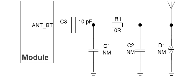
Reference Design
A reference circuit for the RF antenna interface is provided below. For better RF performance, it is recommended to reserve a dual L-type
circuit and add an ESD protection component. Components R1, C1--C3 and D1 should be placed as close to the antenna as possible. C1, C2, and D1 are not mounted by default. The parasitic capacitance of TVS should be less than 0.05 pF, and R1 is recommended to be 0 Ω.
NOTE:
If there is DC power at the antenna ports, C3 must be used for DC-blocking to prevent short circuit to ground. The capacitance value is recommended to be 10 pF, which can be adjusted according to actual requirements. If there is no DC power in the peripheral design, C3 should not be reserved.
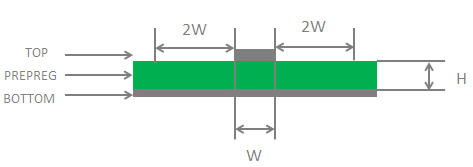
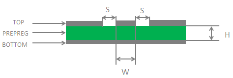
RF Routing Guidelines
For user's PCB, the characteristic impedance of all RF traces should be controlled to 50 Ω. The impedance of the RF traces is usually determined by the trace width (W), the materials' dielectric constant, the height from the reference ground to the signal layer (H), and the spacing between RF traces and grounds (S). Microstrip or coplanar waveguide is typically used in RF layout to control characteristic impedance. The following are reference designs of microstrip or coplanar waveguide with different PCB structures.
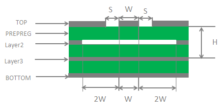
To ensure RF performance and reliability, follow the principles below in RF layout design:
- Use an impedance simulation tool to control the characteristic impedance of RF traces to 50 Ω.
- GND pins adjacent to RF pins should not be designed as thermal relief pads, and should be fully connected to the ground.
- The distance between the RF pins and the RF connector should be as short as possible and all right-angle traces should be changed to curved ones. The recommended trace angle is 135°.
- There should be clearance under the signal pin of the antenna connector or solder joint.
- The reference ground of RF traces should be complete. In addition,adding some ground vias around RF traces and the reference ground could help to improve RF performance. The distance between the ground vias and RF traces should be at least twice the width of RF signal traces (2 × W).
- Keep RF traces away from interference sources (such as DC-DC,(U)SIM/USB/SDIO high frequency digital signals, display signals, and clock signals), and avoid intersection and paralleling between traces on adjacent layers.
For more details about RF layout, see document [3].
PCB Antenna 11
PCB Antenna Specifications:
| Parameter | Specification |
|---|---|
| Frequency Range (GHz) | 2.400--2.500 |
| Input Impedance (Ω) | 50 |
| VSWR | ≤ 4.2 |
| Gain (dBi) | -3.7 (Max.) |
| Efficiency | 18.8 % |
The performance of the PCB antenna depends on the entire product,including the motherboard, case, and other RF signals, and it is
recommended to verify it at the early stage of design. To ensure the performance and reliability when designed with PCB antenna, follow the basic principles below for module's placement and layout:
- The module should be placed on the edge of the motherboard.
- On the motherboard, all PCB layers under the PCB antenna should be designed as keepout areas.
- On the motherboard, ensure a minimum clearance of 16 millimeters between the PCB antenna and vias, traces, copper pour area, and other
components, such as connectors, Ethernet ports and any metal components.
- For the product with a plastic case, ensure a minimum clearance of 10 millimeters between the PCB antenna and the plastic case. For the
product with a metal case, it is recommended to use an external antenna.
NOTE:
If any of the above principles cannot be guaranteed, it is advisable to explore alternative antenna solutions for the module or seek assistance from the Quectel Antenna Team, who can offer design assistance and recommend suitable external antennas. Please feel free to contact Quectel Technical Support if necessary.
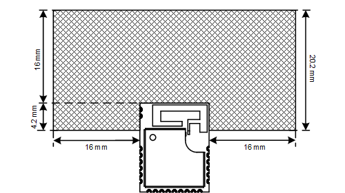
During PCB design, do not route traces across the RF test point at the bottom of the module to ensure the module performance.
RF Coaxial Connector 12
Receptacle Specifications
The module provides 4th generation RF coaxial connector and the mechanical dimensions of the receptacle mounted on the module are as follows.
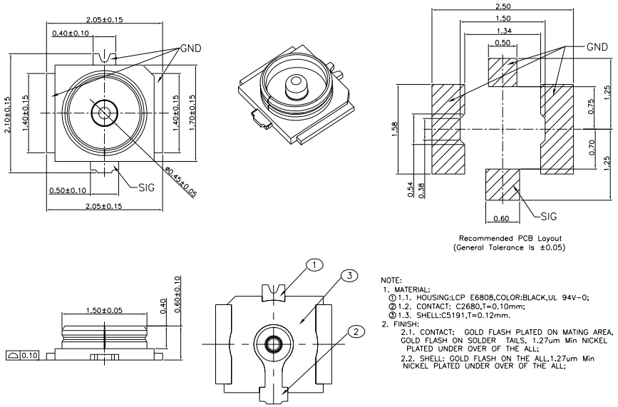
Major Specifications of the Receptacle:
| Item | Specification |
|---|---|
| Nominal Frequency Range | DC to 6 GHz |
| Nominal Impedance | 50 Ω |
| Temperature Rating | -40 °C to +85 °C |
| Voltage Standing Wave Ratio (VSWR) | Meet the requirements of: Max. 1.3 (DC–3 GHz) Max. 1.45 (3–6 GHz) |
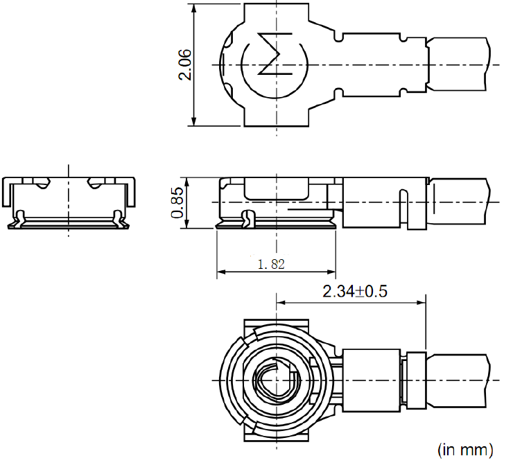
Antenna Connector Installation
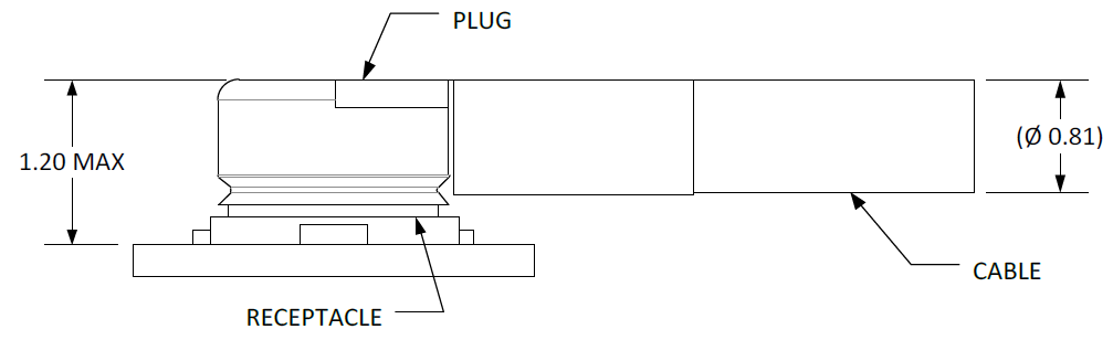
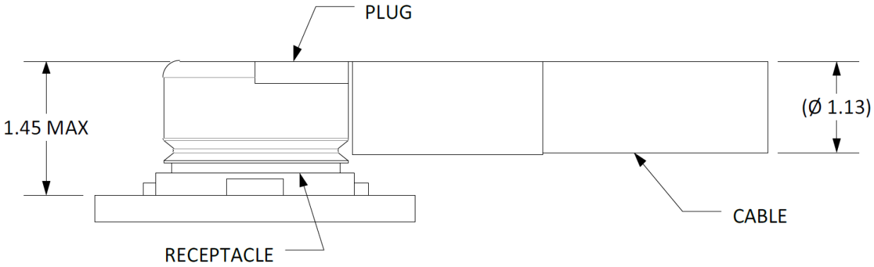
The receptacle mounted on the module accepts two types of mated plugs that will meet a maximum height of 1.2 mm using a Ø 0.81 mm coaxial cable or a maximum height of 1.45 mm utilizing a Ø 1.13 mm coaxial cable.
The following figure shows the dimensions of mated plugs using Ø 0.81 mm coaxial cables.
The following figure illustrates the connection between the receptacle on the module and the mated plug using a Ø 0.81 mm coaxial cable.
The following figure illustrates the connection between the receptacle mounted on the module and the mated plug using a Ø 1.13 mm coaxial cable.
Assemble Coaxial Cable Plug Manually
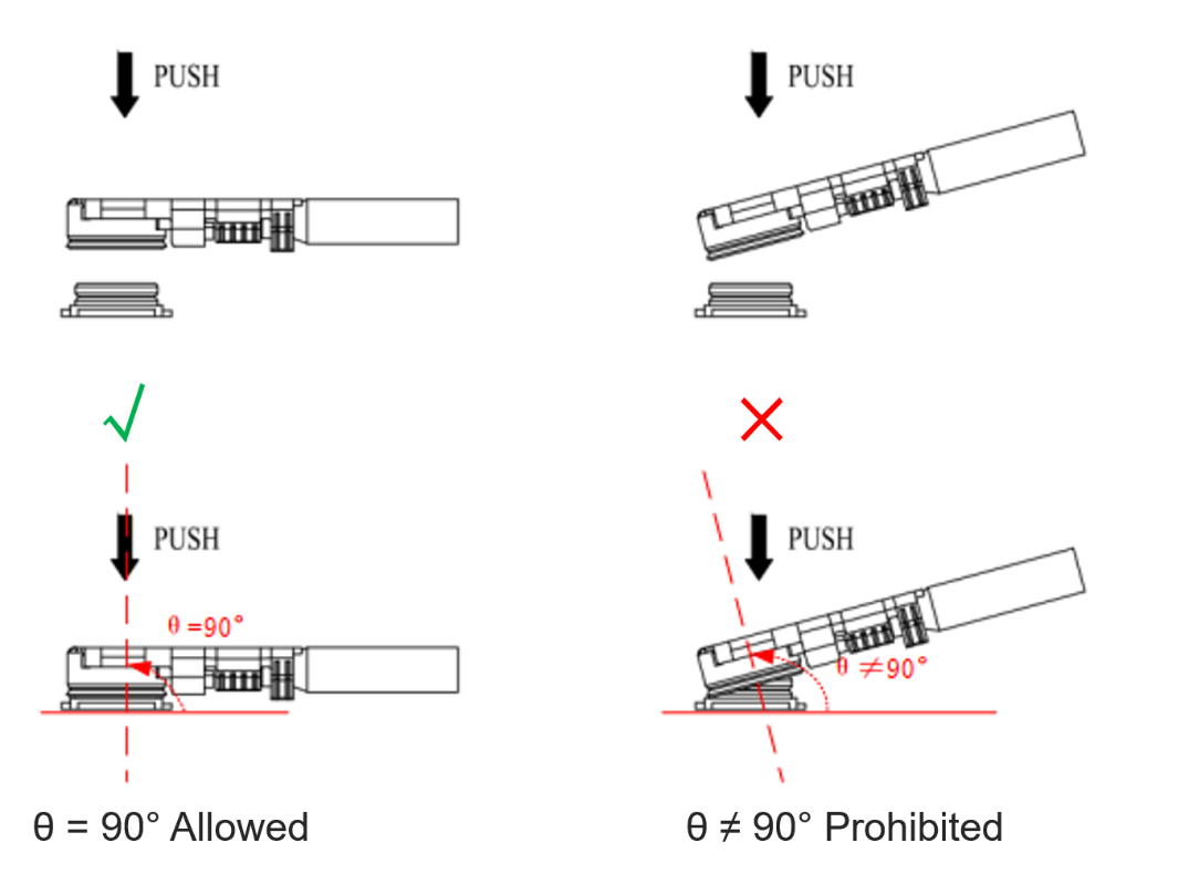
The pictures for plugging in a coaxial cable plug is shown below, θ =90° is acceptable, while θ ≠ 90° is not.
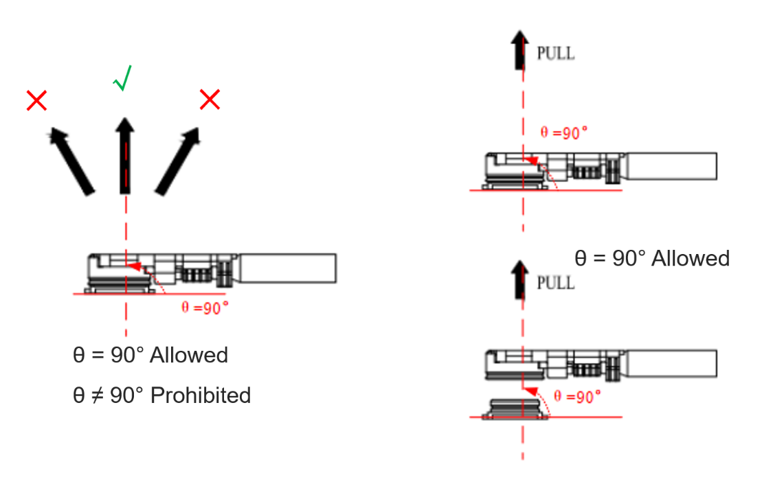
The pictures of pulling out the coaxial cable plug is shown below, θ =90° is acceptable, while θ ≠ 90° is not.
Assemble Coaxial Cable Plug with Jig
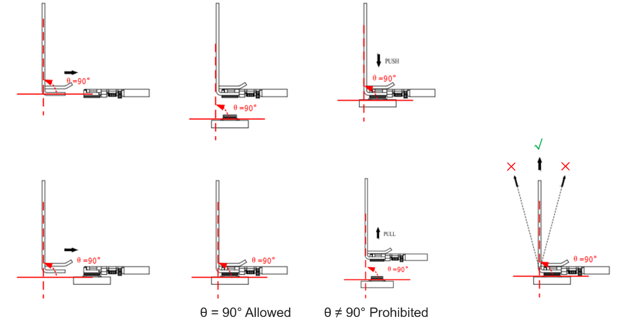
The pictures of installing the coaxial cable plug with a jig is shown below, θ = 90° is acceptable, while θ ≠ 90° is not.
Recommended Mated Plug and Cable Manufacturer
Mated plugs and cables by I-PEX are recommended. For more details, visit https://www.i-pex.com .
Antenna Design Requirements
Antenna Design Requirements:
| Parameter | Requirements |
|---|---|
| Frequency Range (GHz) | 2.4 GHz: 2.400--2.4835 GHz |
| Pin Antenna Interface, RF Coaxial Connector |
Electrical Characteristics & Reliability
Absolute Maximum Ratings
Absolute maximum ratings for power supply and voltage on digital and analog pins of the module are listed in the following table.
Absolute Maximum Ratings (Unit:V):
| Parameter | Min. | Max. |
|---|---|---|
| VBAT | -0.3 | 4.3 |
| VIO | -0.3 | 3.6 |
| Voltage at ADC[0:3] | 0 | 3.6 |
Power Supply Ratings
Module Power Supply Ratings(Unit: V):
| Parameter | Description | Condition | Min. | Typ. | Max. |
|---|---|---|---|---|---|
| VBAT | Power supply for the module | The actual input voltages must be kept between the minimum and maximum values. | 2.4 | 3.3 | 4.3 |
Bluetooth Power Consumption
BLE Power Consumption:
| Mode | Typ. | Max. | Unit |
|---|---|---|---|
| Sleep | 6.2 | - | μA |
| Shutdown | 3.1 | - | μA |
| BLE 1 Mbps @ Tx 10 dBm | - | 21.9 | mA |
Digital I/O Characteristics
I/O Characteristics (Unit: V):
| Parameter | Description | Min. | Max. |
|---|---|---|---|
| VIH | High-level input voltage | 0.7 × VIO | 3.3 |
| VIL | Low-level input voltage | -0.3 | 0.3 × VIO |
| VOH | High-level output voltage | 2.4 | 3.3 |
| VOL | Low-level output voltage | - | 0.4 |
NOTE:
The power supply for the module's I/O ports depends on the VBAT voltage level. When VBAT is greater than 2.9 V, the I/O port voltage
(VIO) can be converted via an internal LDO and defaults to 2.9 V, which can be adjusted through software. When VBAT is less than 2.9 V, the I/O port voltage (VIO) is equal to VBAT.
ESD Protection
Static electricity occurs naturally and may damage the module.Therefore, applying proper ESD countermeasures and handling methods is
imperative. For example, wear anti-static gloves during the development,production, assembly and testing of the module; add ESD protection components to the ESD sensitive interfaces and points in the product design.
ESD Characteristics (Unit: kV):
| Model | Test Result | Standard |
|---|---|---|
| Human Body Model (HBM) | ±4 | ANSI/ESDA/JEDEC JS-001-2017 |
| Charged Device Model (CDM) | ±0.5 | ANSI/ESDA/JEDEC JS-002-2018 |
Mechanical Information
This chapter describes the mechanical dimensions of the module. All dimensions are measured in millimeters (mm), and the dimensional tolerances are ±0.2 mm unless otherwise specified.
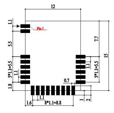
Mechanical Dimensions
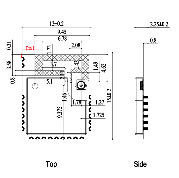
NOTE:
The module's coplanarity standard: ≤ 0.13 mm.
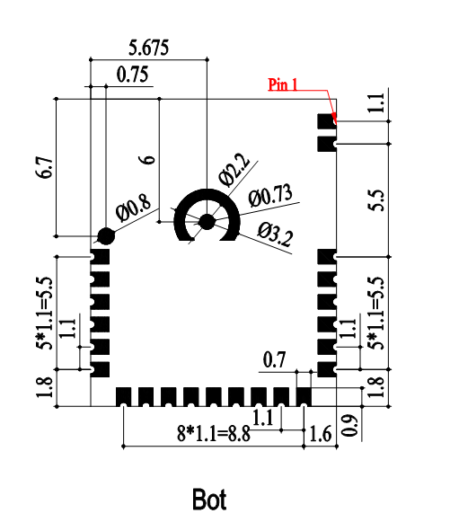
Recommended Footprint
NOTE:
Keep at least 3 mm between the module and other components on the motherboard to improve soldering quality and maintenance convenience.
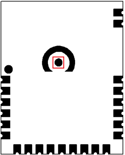
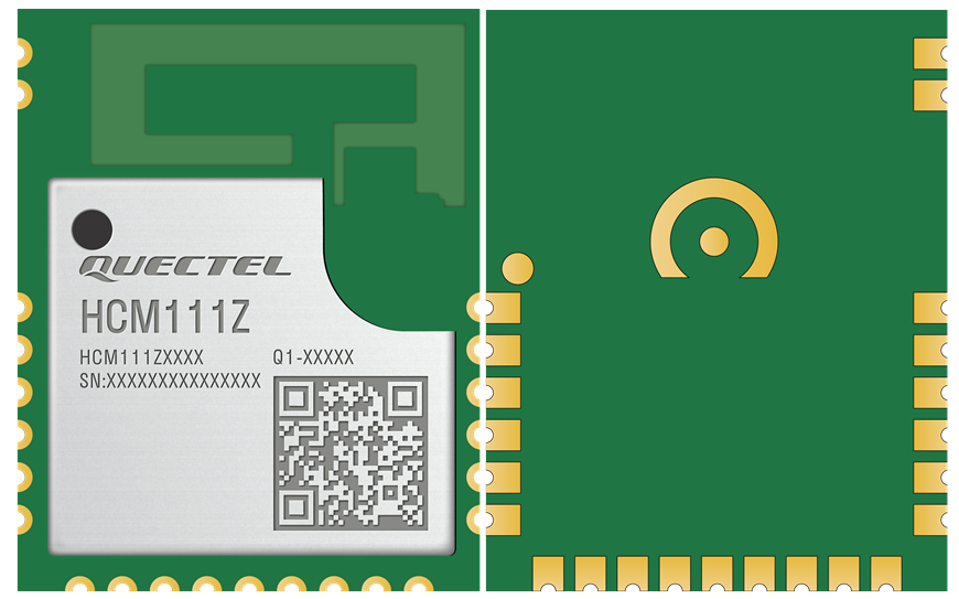
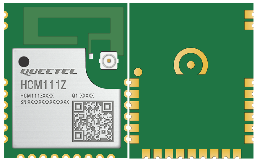
Top and Bottom Views
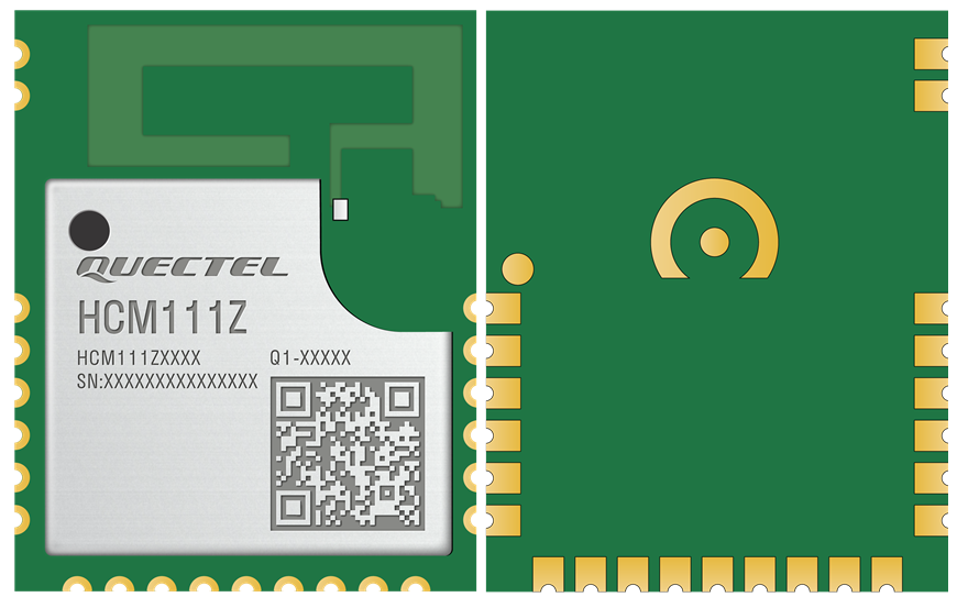
NOTE:
- Images above are for illustrative purposes only and may differ from the actual module. For authentic appearance and label,please refer to the module received from Quectel.
- The RF coaxial connector is not available when the module is designed with pin antenna interface (ANT_BT) or PCB antenna.
Storage and Packaging
Storage Conditions
The module is provided with vacuum-sealed packaging. MSL of the module is rated as 3. The storage requirements are shown below.
- Recommended Storage Condition: the temperature should be 23 ±5 °C and the relative humidity should be 35--60 %.
- Shelf life (in a vacuum-sealed packaging): 12 months in Recommended Storage Condition.
- Floor life: 168 hours 13 in a factory where the temperature is 23±5 °C and relative humidity is below 60 %. After the vacuum-sealed packaging is removed, the module must be processed in reflow soldering or other high-temperature operations within 168 hours.Otherwise, the module should be stored in an environment where the relative humidity is less than 10 % (e.g., a dry cabinet).
- The module should be pre-baked to avoid blistering, cracks and inner-layer separation in PCB under the following circumstances:
- The module is not stored in Recommended Storage Condition;
- Violation of the third requirement mentioned above;
- Vacuum-sealed packaging is broken, or the packaging has been removed for over 24 hours;
- Before module repairing.
- If needed, the pre-baking should follow the requirements below:
- The module should be baked for 24 hours at 120 ±5 °C;
- The module must be soldered to PCB within 24 hours after the baking,otherwise it should be put in a dry environment such as in a dry cabinet.
NOTE:
- To avoid blistering, layer separation and other soldering issues,extended exposure of the module to the air is forbidden.
- Take out the module from the package and put it on high-temperature-resistant fixtures before baking. If shorter baking time is desired, see IPC/JEDEC J-STD-033 for the baking procedure.
- Pay attention to ESD protection, such as wearing anti-static gloves, when touching the modules.
Manufacturing and Soldering
Push the squeegee to apply the solder paste on the surface of stencil,thus making the paste fill the stencil openings and then penetrate to the PCB. Apply proper force on the squeegee to produce a clean stencil surface on a single pass. To guarantee module soldering quality, the thickness of stencil for the module is recommended to be 0.15--0.18 mm.For more details, see document [4].
The recommended peak reflow temperature should be 235--246 ºC, with 246ºC as the absolute maximum reflow temperature. To avoid damage to the module caused by repeated heating, it is recommended that the module should be mounted only after reflow soldering for the other side of PCB has been completed. The recommended reflow soldering thermal profile(lead-free reflow soldering) and related parameters are shown below.
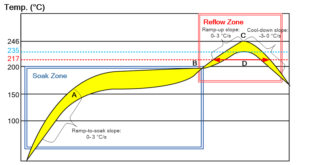
Recommended Thermal Profile Parameters:
| Factor | Recommended Value |
|---|---|
| Soak Zone | |
| Ramp-to-soak slope | 0--3 °C/s |
| Soak time (between A and B: 150 °C and 200 °C) | 70--120 s |
| Reflow Zone | |
| Ramp-up slope | 0--3 °C/s |
| Reflow time (D: over 217 °C) | 40--70 s |
| Max. temperature | 235--246 °C |
| Cool-down slope | -3--0 °C/s |
| Reflow Cycle | |
| Max. reflow cycle | 1 |
NOTE:
- The above profile parameter requirements are for the measured temperature of solder joints. Both the hottest and coldest spots of solder joints on the PCB should meet the above requirements.
- During manufacturing and soldering, or any other processes that may contact the module directly, NEVER wipe the module's shielding can with organic solvents, such as acetone, ethyl alcohol, isopropyl alcohol, trichloroethylene. Otherwise, the shielding can may become rusted.
- The shielding can for the module is made of Cupro-Nickel base material. It is tested that after 12 hours' Neutral Salt Spray test, the laser engraved label information on the shielding can is still clearly identifiable and the QR code is still readable,although white rust may be found.
- If a conformal coating is necessary for the module, do NOT use any coating material that may chemically react with the PCB or shielding cover, and prevent the coating material from flowing into the module.
- Avoid using ultrasonic technology for module cleaning since it can damage crystals inside the module.
- Avoid using materials that contain mercury (Hg), such as adhesives, for module processing, even if the materials are RoHS compliant and their mercury content is below 1000 ppm (0.1 %).
- Corrosive gases may corrode the electronic components inside the module, affecting their reliability and performance, and potentially leading to a shortened service life that fails to meet the designed lifespan. Therefore, do not store or use unprotected modules in environments containing corrosive gases such as hydrogen sulfide, sulfur dioxide, chlorine, and ammonia.
- Due to the complexity of the SMT process, please contact Quectel Technical Support in advance for any situation that you are not sure about, or any process (e.g. selective soldering, ultrasonic soldering) that is not mentioned in document [5].
Packaging Specification
This chapter outlines the key packaging parameters and processes. All figures below are for reference purposes only, as the actual appearance and structure of packaging materials may vary in delivery.
The modules are packed in a tape and reel packaging as specified in the sub-chapters below.
Carrier Tape
Carrier tape dimensions are illustrated in the following figure and table:
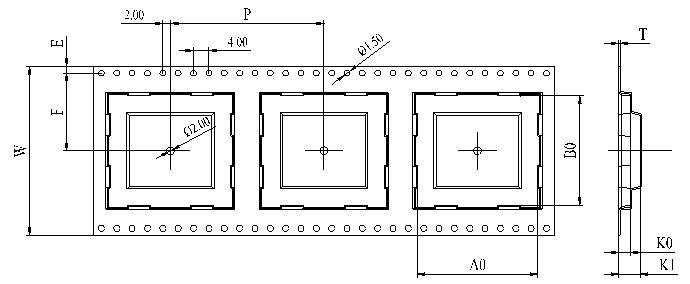
Carrier Tape Dimension Table(Unit: mm):
| W | P | T | A0 | B0 | K0 | K1 | F | E |
|---|---|---|---|---|---|---|---|---|
| 32 | 20 | 0.4 | 12.4 | 15.4 | 2.75 | 3.8 | 14.2 | 1.75 |
Plastic Reel
Plastic reel dimensions are illustrated in the following figure and table:
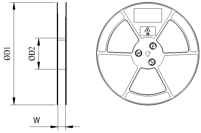
Plastic Reel Dimension Table(Unit: mm):
| øD1 | øD2 | W |
|---|---|---|
| 380 | 100 | 32.5 |
Mounting Direction
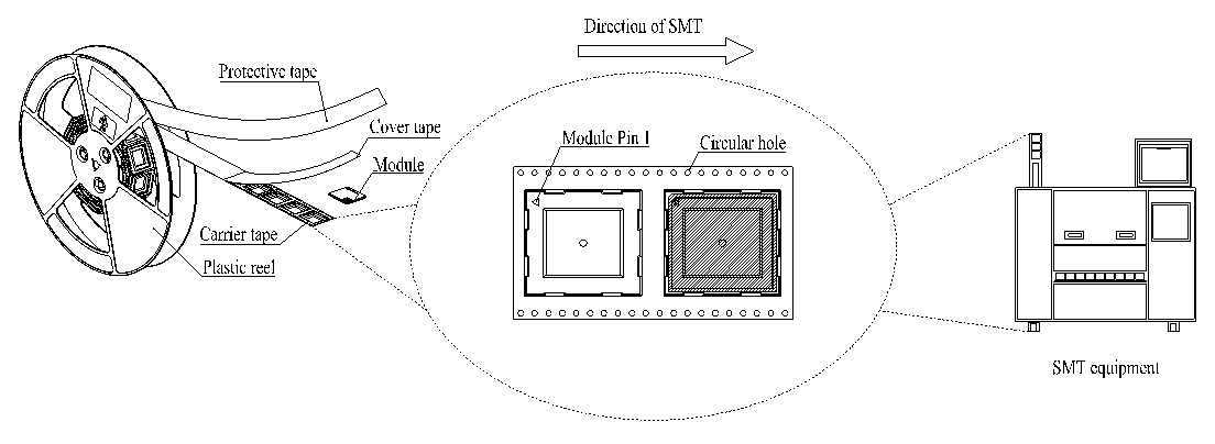
Packaging Process
Packaging Process:
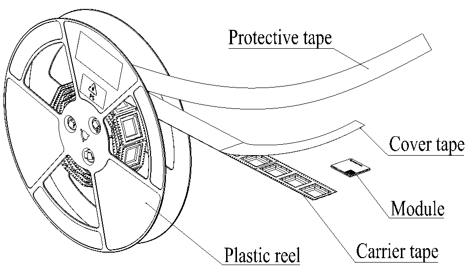
Place the modules onto the carrier tape cavity and cover them securely with cover tape. Wind the heat-sealed carrier tape onto a plastic reel and apply a protective tape for additional protection. 1 plastic reel can pack 1000 modules.
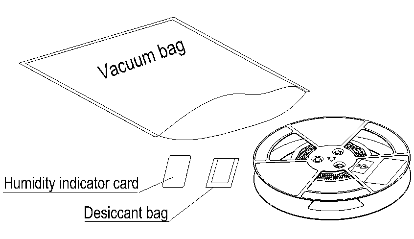
Place the packaged plastic reel, humidity indicator card and desiccant bag into a vacuum bag, and vacuumize it.
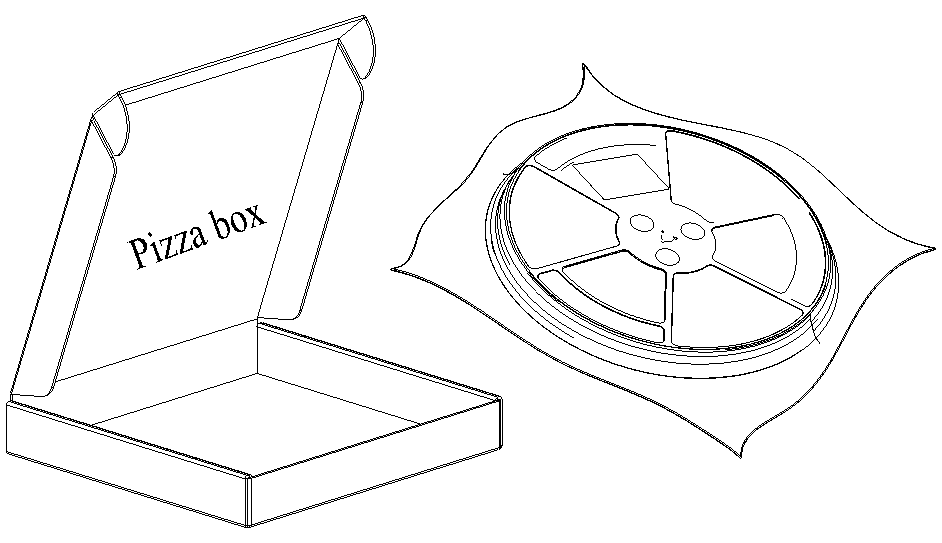
Place the vacuum-packed plastic reel into a pizza box.
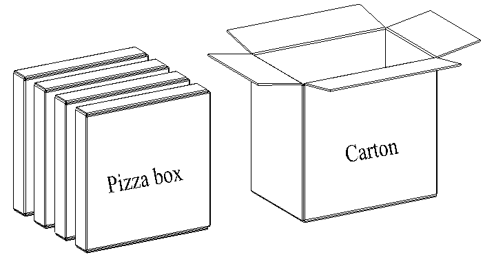
Put the 4 packaged pizza boxes into 1 carton and seal it. 1 carton can pack 4000 modules.
Appendix References
Reference Documents:
| Document Name |
|---|
| [1] Quectel_HCM111Z_TE-B_User_Guide |
| [2] Quectel_HCM111Z_AT_Command_Manual |
| [3] Quectel_RF_Layout_Application_Note |
| [4] Quectel_Module_Stencil_Design_Requirements |
| [5] Quectel_Module_SMT_Application_Note |
Terms and Abbreviations:
| Abbreviation | Description |
|---|---|
| ADC | Analog-to-Digital Converter |
| AMMBA | Advanced Microcontroller Bus Architecture |
| APB | Advanced Peripheral Bus |
| ARM | Advanced RISC Machine |
| BLE | Bluetooth Low Energy |
| CDM | Charged Device Model |
| DAC | Digital-to-Analog Converter |
| DSP | Digital Signal Processor |
| ESD | Electrostatic Discharge |
| GFSK | Gauss Frequency Shift Keying |
| GND | Ground |
| GPIO | General-Purpose Input/Output |
| HBM | Human Body Model |
| I/O | Input/Output |
| I2C | Inter-Integrated Circuit |
| I2S | Inter-IC Sound |
| LCC | Leadless Chip Carrier |
| Mbps | Megabits per second |
| MCU | Microcontroller Unit |
| NM | Not Mounted |
| OTA | Over The Air |
| PCB | Printed Circuit Board |
| PCM | Pulse Code Modulation |
| PWM | Pulse Width Modulation |
| RF | Radio Frequency |
| RoHS | Restriction of Hazardous Substances |
| SDIO | Secure Digital Input/Output |
| SPI | Serial Peripheral Interface |
| SRAM | Static Random-Access Memory |
| SWD | Serial Wire Debug |
| TVS | Transient Voltage Suppressor |
| UART | Universal Asynchronous Receiver/Transmitter |
| USB | Universal Serial Bus |
| (U)SIM | (Universal) Subscriber Identity Module |
| VIH | High-level Input Voltage |
| VIL | Low-level Input Voltage |
| Vmax | Maximum Voltage |
| Vmin | Minimum Voltage |
| Vnom | Normal Voltage Value |
| VOH | High-level Output Voltage |
| VOL | Low-level Output Voltage |
| VSWR | Voltage Standing Wave Ratio |
Within the operating temperature range, the module's related performance meets Bluetooth specifications.↩
For more details about the TE-B, see document [1].↩
The module is provided with one of the three antenna/antenna interface designs. For more details, contact Quectel Technical Support.↩
For more details about the interfaces, see Chapter 3.3 andChapter 3.4.↩
The power supply for the module's I/O ports depends on the VBAT voltage level. When VBAT is greater than 2.9 V, the I/O port voltage(VIO) can be converted via an internal LDO and defaults to 2.9 V,which can be adjusted through software. When VBAT is less than 2.9V, the I/O port voltage (VIO) is equal to VBAT. For the I/O characteristics, please refer to Table 26. For more details, contact Quectel Technical Support.↩
Pin 10 is configured as "sleep wake-up control" and set to a high level by default in the standard firmware, and pull it low to go into sleep mode and pull it high to wake up the module.↩
Pin 22 is configurated as "message notification indication" and set to a high level by default in the standard firmware, and pull it low to enable the message notification. For more details, seedocument [2].↩
The analog audio interfaces are optional. If unused, keep them open. For more details, contact Quectel Technical Support.↩
The analog audio interfaces are optional. If unused, keep them open. For more details, contact Quectel Technical Support.↩
The module is provided with one of the three antenna/antenna interface designs. For more details, contact Quectel Technical Support.↩
The module is provided with one of the three antenna/antenna interface designs. For more details, contact Quectel Technical Support.↩
The module is provided with one of the three antenna/antenna interface designs. For more details, contact Quectel Technical Support.↩
This floor life is only applicable when the environment conforms to IPC/JEDEC J-STD-033. It is recommended to start the solder reflow process within 24 hours after the package is removed if the temperature and moisture do not conform to, or are not sure to conform to IPC/JEDEC J-STD-033. Do not unpack the modules in large quantities until they are ready for soldering.↩