

 English
FC41D TE-B User Guide
Introduction
For convenient development of applications with FC41D module in QuecOpen® solution, Quectel supplies the corresponding development board (FC41D-TE-B) for the module testing. This document provides a quick insight into FC41D-TE-B interface specifications, RF characteristics, electrical and mechanical details and explains how to use it.
General Overview
FC41D-TE-B is a development board that supports a series of interfaces. It can be used for testing basic functionalities or further development of the module.
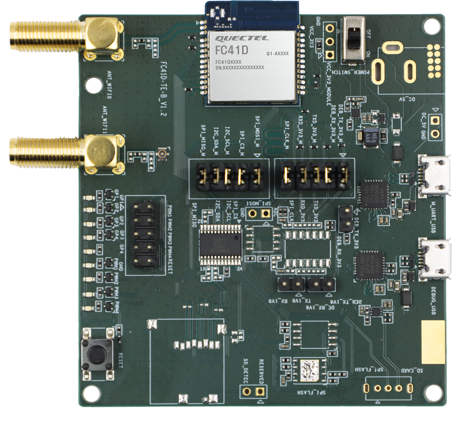
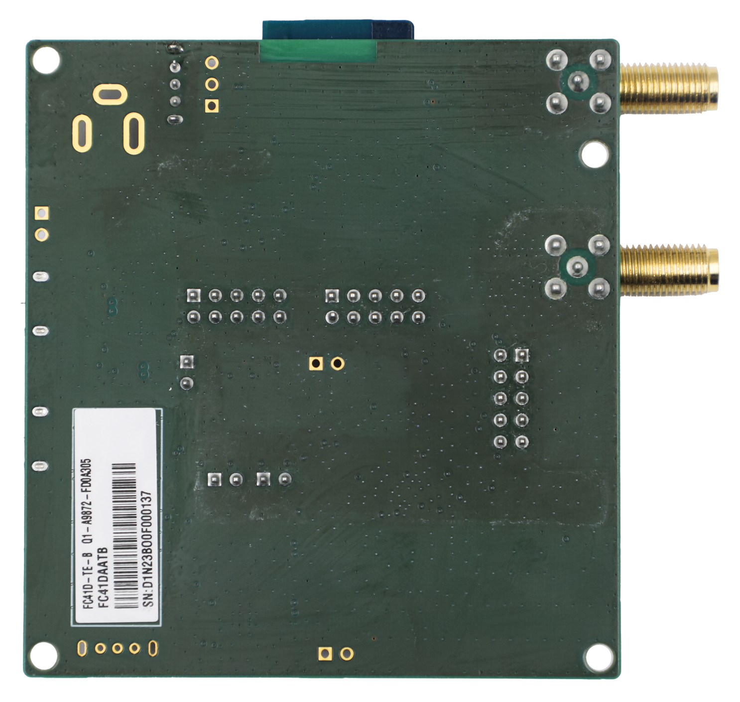
Top and Bottom Views
Component Placement
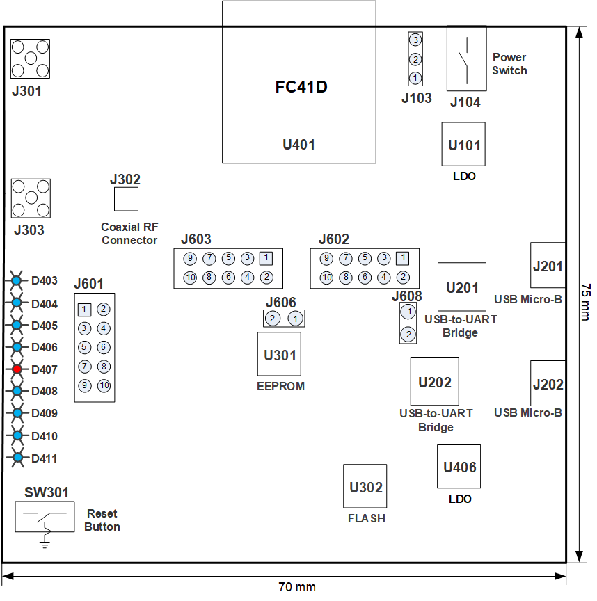
Interfaces of FC41D-TE-B:
| Interface | Reference No. | Description |
|---|---|---|
| Power Supply Interfaces | J201, J202 | |
| Power Switch | J104 | VBAT ON/OFF control |
| Reset Button | SW301 | Used for resetting the module |
| USB Connectors | J201 | Connect to main UART interface of the module via USB-to-UART bridge U201 |
| USB Connectors | J202 | Connect to debug UART interface of the module via USB-to-UART bridge U202 |
| RF Connectors | J301 | SMA connector of the module ANT_WIFI/BT pin |
| RF Connectors | J302 | Coaxial RF connector |
| RF Connectors | J303 | SMA connector of the module's coaxial RF connector |
| Status LEDs | D403 | GPIO1 status indicator |
| Status LEDs | D404 | GPIO2 status indicator |
| Status LEDs | D405 | GPIO3 status indicator |
| Status LEDs | D406 | GPIO4 status indicator |
| Status LEDs | D407 | VBAT ON/OFF indicator |
| Status LEDs | D408 | PWM1 status indicator |
| Status LEDs | D409 | PWM2 status indicator |
| Status LEDs | D410 | PWM3 status indicator |
| Status LEDs | D411 | PWM4 status indicator |
| Test Points | J103, J601, J602, J603 | Test pins |
| Analog Signal Input Interface | J606 | Used for inputting an external analog signal into ADC pin of the module |
| Mode Selection | J608 | - With jumper, the module enters RF test mode - Without jumper, the module enters normal mode by default |
NOTE:
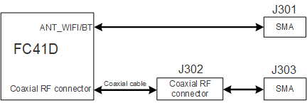
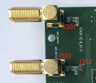
The ANT_WIFI/BT pin antenna and coaxial RF connector are optional for the module. J301 is used for the module's ANT_WIFI/BT pin, and J302 and J303 are used for the module's coaxial RF connector.
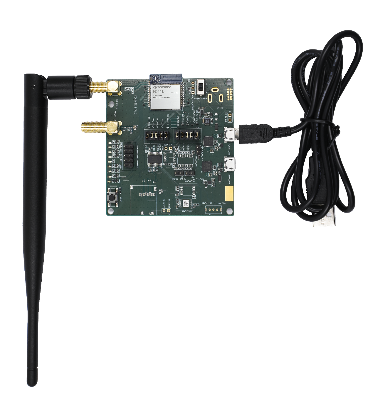
Kit Accessories & Assembly
Kit Accessories
Accessories List:
| Items | Description | Quantity(pcs) |
|---|---|---|
| Cables | USB micro-B cable | 2 |
| Cables | Coaxial cable | 1 |
| Antennas | Wi-Fi&Bluetooth antenna | 2 |
| Instruction Sheet | A sheet of paper giving instructions for TE-B connection, details of TE-B accessories, etc. | 1 |
Kit Assembly
The connection between the TE-B and its components is shown in the figure below. Refer to the instruction sheet in the accessories list for more details.
Interface Applications
This chapter outlines the information and applications of some hardware interfaces of FC41D-TE-B.
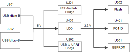
Power Supply Interfaces
FC41D-TE-B can be powered by USB Micro-B connectors (J201, J202).
The simplified power supply schematic of FC41D-TE-B is provided in the following figure.
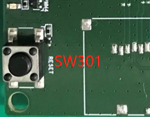
Power Switch and Reset Button
FC41D-TE-B includes one power switch (J104) and one reset button (SW301) as shown in the following figure.
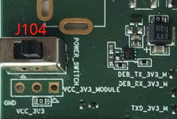
Description of Power Switch and Reset Button:
| Reference No. | Description |
|---|---|
| J104 | VBAT ON/OFF control |
| SW301 | Used for resetting the module |
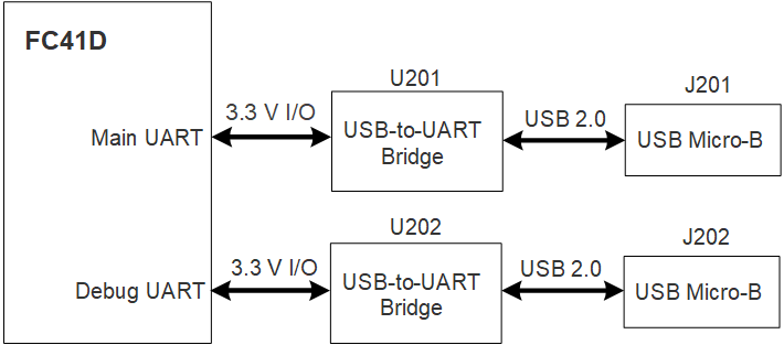
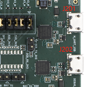
USB Connectors
FC41D-TE-B features two USB connectors, J201 and J202, which are connected to the main UART and debug UART interfaces of the module via U201 and U202 respectively.
J201 supports 115200 bps baud rate by default. It is intended for data transmission between the module and the host application. It can be used for firmware downloading and AT command communication.
J202 supports 921600 bps baud rate by default. It can be used for outputting partial logs.
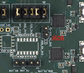
Mode Selection
FC41D-TE-B offers a two-pin header J608 for selecting the operating mode. the module enters RF test mode with the jumper. Otherwise, it enters normal mode.
RF Connectors
FC41D-TE-B features two SMA connectors (J301, J303). The ANT_WIFI/BT pin antenna and coaxial RF connector are optional for the module. You can connect coaxial RF connector of the module to J302 through coaxial cable, then the module RF signal can be tested via an external antenna or instrument on J303. Also, you can connect ANT_WIFI/BT pin to J301.
Block diagram of RF connectors is illustrated in the figure below.
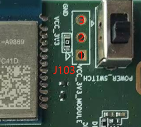
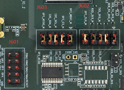
Test Points
FC41D-TE-B features a series of test points, which can help you to obtain the corresponding waveform of some signals.
J103, J601, J602 and J603 test points are illustrated in the following figures.
Pin Definition of J103, J601, J602, J603:
J103:
| Pin No. | Pin Name | Description |
|---|---|---|
| 1 | UVCC_3V3_MODULE | VBAT power supply of the module |
| 2 | VCC_3V3 | 3.3 V power supply |
| 3 | GND | Ground |
J601:
| Pin No. | Pin Name | Description |
|---|---|---|
| 1 | GPIO1 | Connected directly to GPIO1 of the module |
| 2 | PWM1 | Connected directly to PWM1 of the module |
| 3 | GPIO2 | Connected directly to GPIO2 of the module |
| 4 | PWM2 | Connected directly to PWM2 of the module |
| 5 | GPIO3 | Connected directly to GPIO3 of the module |
| 6 | PWM3 | Connected directly to PWM3 of the module |
| 7 | GPIO4 | Connected directly to GPIO4 of the module |
| 8 | PWM4 | Connected directly to PWM4 of the module |
| 9 | GND | Ground |
| 10 | RESET | Connected directly to CEN of the module |
J602:
| Pin No. | Pin Name | Description |
|---|---|---|
| 1 | DEB_TX_3V3_M | Connected directly to DBG_TXD of the module |
| 2 | DEB_TX_3V3 | Connected directly to UART_RXD of U202 |
| 3 | DEB_RX_3V3_M | Connected directly to DBG_RXD of the module |
| 4 | DEB_RX_3V3 | Connected directly to UART_TXD of U202 |
| 5 | TXD_3V3_M | Connected directly to MAIN_TXD of the module |
| 6 | TXD_3V3 | Connected directly to UART_RXD of U201 |
| 7 | RXD_3V3_M | Connected directly to MAIN_RXD of the module |
| 8 | RXD_3V3 | Connected directly to UART_TXD of U201 |
| 9 | SPI_CLK_M | Connected directly to SPI_CLK of the module |
| 10 | SPI_CLK | Connected directly to SPI_CLK of U302 via a multiplexer |
J603:
| Pin No. | Pin Name | Description |
|---|---|---|
| 1 | SPI_MOSI_M | Connected directly to SPI_MOSI of the module |
| 2 | SPI_MOSI | Connected to SPI_MOSI of U302 via a multiplexer |
| 3 | SPI_CS_M | Connected directly to SPI_CS of the module |
| 4 | SPI_CS | Connected to SPI_CS of U302 via a multiplexer |
| 5 | I2C_SCL_M | Connected directly to I2C_SCL of the module |
| 6 | I2C_SCL | Connected directly to I2C_SCL of U301 |
| 7 | I2C_SDA_M | Connected directly to I2C_SDA of the module |
| 8 | I2C_SDA | Connected directly to I2C_SDA of U301 |
| 9 | SPI_MISO_M | Connected directly to SPI_MISO of the module |
| 10 | SPI_MISO | Connected to SPI_MISO of U302 via a multiplexer |
NOTE:
See document [1] for details of the module pin name and definition in the above table.
Analog Signal Input Interface
FC41D-TE-B provides an analog signal input interface, which is connected to the ADC pin of the module. The position of the input interface is presented in the following figure.
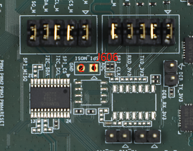
Pin Definition of J606:
J606:
| Pin No. | Pin Name | Description |
|---|---|---|
| 1 | ADC | Analog signal input pin |
| 2 | GND | Ground |
Status LEDs
FC41D-TE-B comprises 9 status LEDs. The positions of these LED indicators are presented in the following figure.
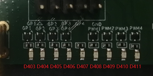
Status LEDs:
| Reference No. | Description |
|---|---|
| D403 | Indicates the status of GPIO1: Light on:high level Light off:low level |
| D404 | Indicates the status of GPIO2: Light on:high level Light off:low level |
| D405 | Indicates the status of GPIO3: Light on: high level Light off:low level |
| D406 | Indicates the status of GPIO4: Light on:high level Light off:low level |
| D407 | VBAT ON/OFF indicator: Light on:VBAT on Light off:VBAT off |
| D408 | Indicates the status of PWM1: Light on:high level Light off:low level |
| D409 | Indicates the status of PWM2: Light on:high level Light off:low level |
| D410 | Indicates the status of PWM3: Light on:high level:Light off - low level |
| D411 | Indicates the status of PWM4: Light on: high level Light off - low level |
Operating Procedures
This chapter outlines how to use the FC41D-TE-B for testing and evaluating the module.
Power Up
- Connect the USB connectors of FC41D-TE-B to PC with the USB micro-B cable.
- Switch J104 (Power Switch) to ON state, then D407 (VBAT ON/OFF indicator) will light up.
Communication via USB Connectors
- Turn on the module according to the procedure mentioned in the Power Up section.
- The USB serial port number can be viewed through the PC Device Manager, as shown below.
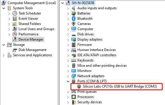
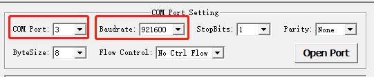
- Use the QCOM tool provided by Quectel to establish communication between the module and the PC via debug UART. Select the "COM port" (USB serial port) and set the correct "Baudrate". For more details about QCOM tool usage and configuration, see the document[2].
Firmware Upgrade
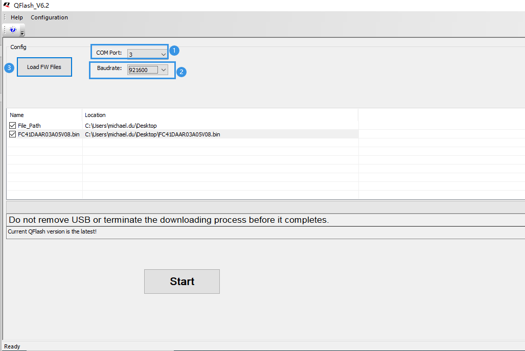
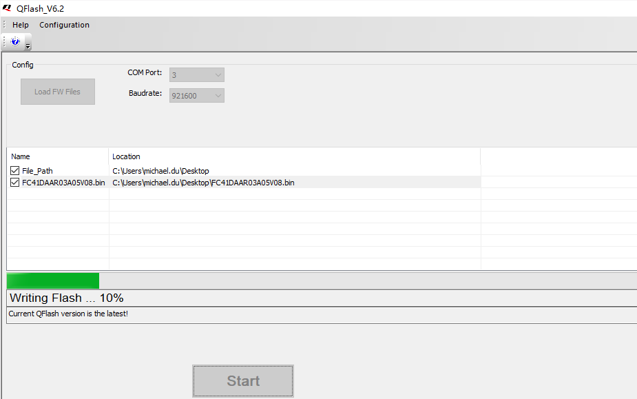
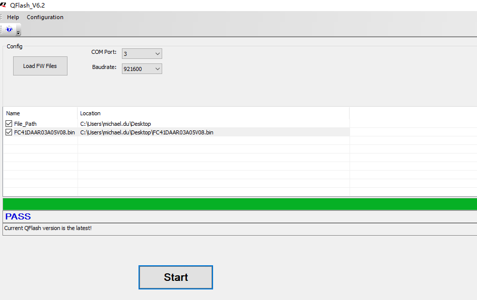
You can use the QFlash tool provided by Quectel to establish communication between the module and the PC via main UART. The module upgrades firmware via main UART with specific steps as below:
- Open the firmware upgrade tool QFlash tool on your PC, and power up the module as explained in the Chapter 5.1.
- Select the main UART port from "COM Port" dropdown list, and select "921600" baud rate from "Baudrate" dropdown list.
- Choose the firmware package from "Load FW Files".
- Click "Start", and then the message "Wait Port (3) is normal ..." appears in the tool window. Press SW301 (reset button) on FC41D-TE-B to upgrade firmware when the message "Erasing Flash ..." appears in the tool window.
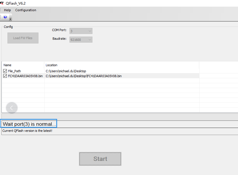
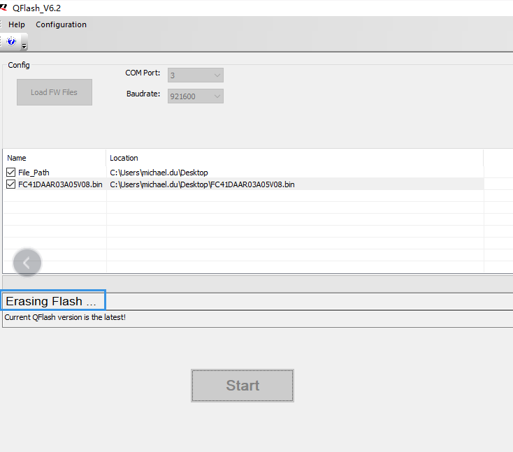
- Firmware is upgrading presenting in percentage form, and "PASS" is displayed in the tool window when the upgrade is completed.
NOTE:
Contact Quectel Technical Support for the QFlash tool and the QFlash version should be later than 5.4. For more details about QFlash tool usage and configuration, see the document[3].
Reset
Press SW301 (reset button) for more than 100 ms and then release it to reset the module.
Appendix References
Related Documents:
| Document Name |
|---|
| [1] Quectel_FC41D_QuecOpen_Hardware_Design |
| [2] Quectel_QCOM_User_Guide |
| [3] Quectel_QFlash_User_Guide |
Terms and Abbreviations:
| Abbreviation | Description |
|---|---|
| ADC | Analog-to-Digital Converter |
| COM | Communication |
| EVB | Evaluation Board |
| EEPROM | Electrically-Erasable Programmable Read-Only Memory |
| GND | Ground |
| GPIO | General Purpose Input/Output |
| LED | Light Emitting Diode |
| NC | Not Connected |
| PC | Personal Computer |
| RF | Radio Frequency |
| SMA | Sub Miniature version A |
| UART | Universal Asynchronous Receiver & Transmitter |
| USB | Universal Serial Bus |