

 English
FC41D Hardware Design
Introduction
This document defines the FC41D and describes its air interface and hardware interfaces which are connected with your application.
With this document, you can quickly understand module interface specifications, electrical and mechanical details, as well as other related information of the module. The document, coupled with application notes and user guides makes it easy to design and set up mobile applications with the module.
Special Mark
Special Mark:
| Mark | Definition |
|---|---|
| * | When an asterisk (*) is used after a function feature,interface, pin name, AT command, or argument, it indicates that the function, feature, interface, pin name, AT command, or argument is under development and currently not supported,unless otherwise specified. |
Product Concept
General Description
FC41D is a low-power, cost-effective Bluetooth 5.2 and IEEE 802.11b/g/n module, which integrates the hardware and software resources required for Wi-Fi and Bluetooth applications. It can support AP and STA of Wi-Fi connection, and low-power Bluetooth connection. It is very suitable for low-speed applications and data acquisition applications such as home intelligent terminal, industrial application and so on.
FC41D has a built-in Wi-Fi and Bluetooth ultra-high integration microcontroller, which provides the necessary ability to calculate and stable Wi-Fi and Bluetooth connectivity for IoT data terminals. It includes:
- 120 MHz ARM kernel
- 256 KB RAM
- 2/4 MB Flash
- Complies with IEEE 802.11b/g/n and Bluetooth 5.2 standards
Key Features
The following table describes the key features of FC41D.
Key Features:
| Features | Details |
|---|---|
| Power Supply | VBAT Power Supply: |
| Operating Frequencies | |
| Wi-Fi Transmission Data Rates | |
| Wi-Fi Transmitting Power | 2.4 GHz: |
| Wi-Fi Protocols | IEEE 802.11b/g/n |
| Wi-Fi Modulations | CCK, BPSK, QPSK,16QAM, 64QAM |
| Wi-Fi Operation Modes | |
| Bluetooth Protocol | Bluetooth 5.2 |
| Bluetooth Operation Mode | BLE |
| Bluetooth Modulation | GFSK |
| Wireless Application Interfaces | |
| Antenna Interfaces | |
| Physical Characteristics | |
| Temperature Ranges | |
| RoHS | All hardware components are fully compliant with EU RoHS directive |
Functional Diagram
The following figure shows a block diagram of FC41D.
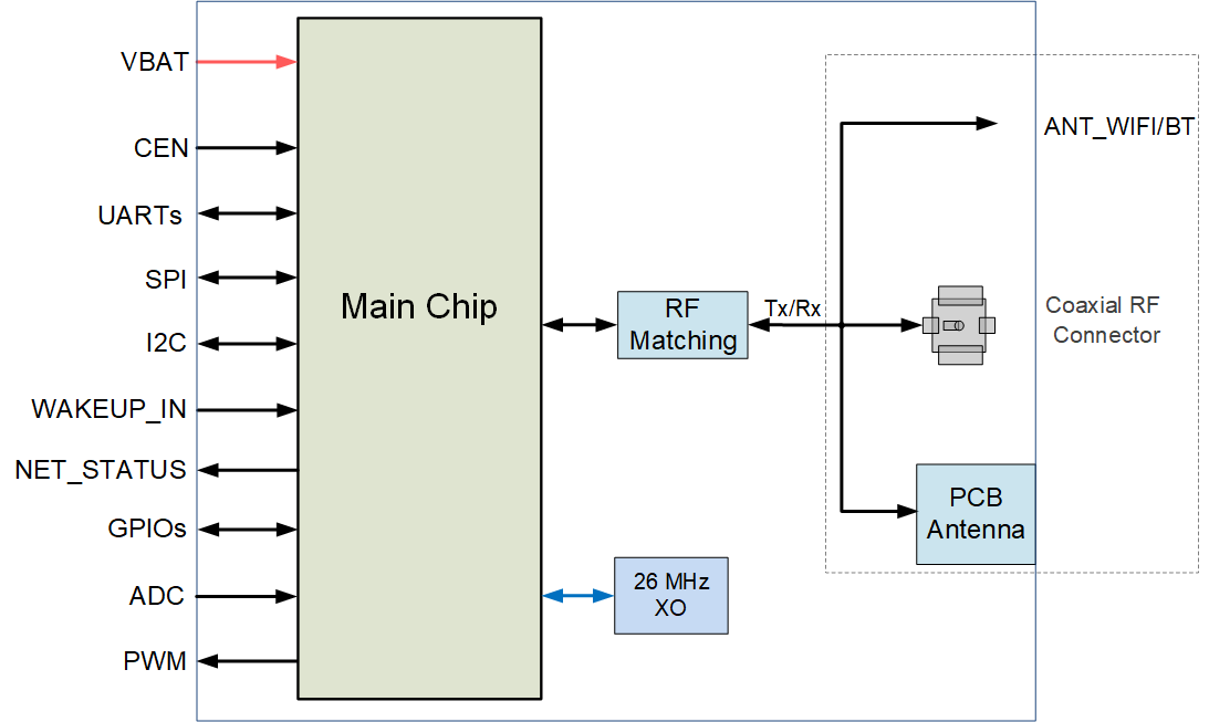
NOTE:
FC41D supports PCB antenna by default; Coaxial RF connector and ANT_WIFI/BT are optional.
EVB Kit
Quectel supplies an evaluation board (FC41D TE-B) with accessories to control or test the module. For more details, see *document[1]*.
Application Interfaces
General Description
The FC41D has 27 LCC pins. The following interfaces are described in detail in subsequent chapters:
- Power supply
- Module reset
- Wireless application interfaces
- UARTs
- SPI* - I2C interface*
- PWM interface*
- WAKEUP interface
- Network status indication
- GPIO interfaces*
- ADC interface*
- RF antenna interfaces
Pin Assignment
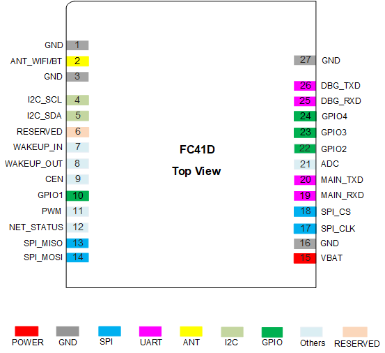
NOTE:
- Keep all RESERVED and unused pins open.
- All GND pins should be connected to ground.
Pin Description
The following tables show the pin description of module.
I/O Parameter Description:
| Type | Description |
|---|---|
| AI | Analog Input |
| AIO | Analog Input/Output |
| DI | Digital Input |
| DIO | Digital Input/Output |
| DO | Digital Output |
| OD | Open Drain |
| PI | Power Input |
Pin Description:
Power Supply:
| Pin Name | Pin No. | I/O | Description | DC Characteristics | Comment |
|---|---|---|---|---|---|
| VBAT | 15 | PI | Power supply for the module | Vmax = 3.6 V Vmin = 3.0 V Vnom = 3.3 V |
It must be provided with sufficient current up to 0.3 A. |
| GND | 1, 3, 16, 27 |
Reset:
| Pin Name | Pin No. | I/O | Description | DC Characteristics | Comment |
|---|---|---|---|---|---|
| CEN | 9 | DI | Resets the module | Vmax = 3.6 V Vmin = 3.0 V Vnom = 3.3 V |
Internally pulled up to 3.3 V. Hardware reset; active low. |
Main UART:
| Pin Name | Pin No. | I/O | Description | DC Characteristics | Comment |
|---|---|---|---|---|---|
| MAIN_TXD | 20 | DO | Main UART transmits | 3.3 V | |
| MAIN_RXD | 19 | DI | Main UART receives | 3.3 V |
Debug UART:
| Pin Name | Pin No. | I/O | Description | DC Characteristics | Comment |
|---|---|---|---|---|---|
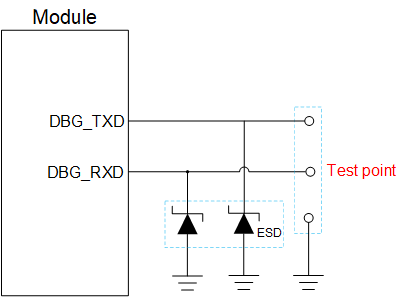
| DBG_TXD | 26 | DO | Debug UART transmits | 3.3 V | Test points must be reserved. |
| DBG_RXD | 25 | DI | Debug UART receives | 3.3V | Test points must be reserved. |
SPI*:
| Pin Name | Pin No. | I/O | Description | DC Characteristics | Comment |
|---|---|---|---|---|---|
| SPI_MISO | 13 | DIO | SPI master input salve output | 3.3 V | |
| SPI_MOSI | 14 | DIO | SPI master output slave input | 3.3V | |
| SPI_CLK | 17 | DIO | SPI clock | 3.3V | In master mode, it’s an output signal; in slave mode, it’s an input signal. |
| SPI_CS | 18 | DIO | SPI chip select | 3.3V | In master mode, it’s an input signal; in slave mode, it’s an output signal. |
I2C Interface:
| Pin Name | Pin No. | I/O | Description | DC Characteristics | Comment |
|---|---|---|---|---|---|
| I2C_SCL | 4 | OD | I2C serial clock | 3.3 V | Requires external pull-up to 3.3 V. |
| I2C_SDA | 5 | OD | I2C serial data | 3.3V | Requires external pull-up to 3.3 V. |
WAKEUP Interface:
| Pin Name | Pin No. | I/O | Description | DC Characteristics | Comment |
|---|---|---|---|---|---|
| WAKEUP_IN | 7 | DI | Wakes up the module from deep sleep or standby mode | 3.3 V | Rising edge wakeup. |
| WAKEUP_OUT | 8 | DO | Wakes up the host | 3.3V | Active high. |
Indication Interface:
| Pin Name | Pin No. | I/O | Description | DC Characteristics | Comment |
|---|---|---|---|---|---|
| NET_STATUS | 12 | DO | Indicates the module's network activity status | 3.3 V | Outputs high level when Wi-Fi is connected in STA mode. |
PWM Interface:*
| Pin Name | Pin No. | I/O | Description | DC Characteristics | Comment |
|---|---|---|---|---|---|
| PWM | 11 | DO | Pulse width modulation output channel | 3.3 V |
GPIO Interface:*
| Pin Name | Pin No. | I/O | Description | DC Characteristics | Comment |
|---|---|---|---|---|---|
| GPIO1 | 10 | DIO | General-purpose input/output | 3.3 V | Wake-up interrupt. |
| GPIO2 | 22 | DIO | General-purpose input/output | 3.3V | Wake-up interrupt. |
| GPIO3 | 23 | DIO | General-purpose input/output | 3.3V | Wake-up interrupt. |
| GPIO4 | 24 | DIO | General-purpose input/output | 3.3V | Wake-up interrupt. |
ADC Interface:*
| Pin Name | Pin No. | I/O | Description | DC Characteristics | Comment |
|---|---|---|---|---|---|
| ADC | 21 | AI | General-purpose ADC interface | Voltage range: 0–2.4 V |
RF Antenna Interface:
| Pin Name | Pin No. | I/O | Description | DC Characteristics | Comment |
|---|---|---|---|---|---|
| ANT_WIFI/BT | 2 | AIO | Wi-Fi/Bluetooth antenna interface | 50 Ω impedance. |
RESERVED Pin:
| Pin Name | Pin No. | Comment |
|---|---|---|
| RESERVED | 6 | Keep it open. |
Power Supply
The following table shows the definition of power supply and ground pins of FC41D.
Pin Definition of Power Supply and GND Pins:
| Pin Name | Pin No. | I/O | Description | Min. | Typ. | Max. | Unit |
|---|---|---|---|---|---|---|---|
| VBAT | 15 | PI | Power supply for the module | 3.0 | 3.3 | 3.6 | V |
| GND | 1, 3, 16, 27 |
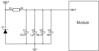
FC41D is powered by VBAT, and it is recommended to use a power supply chip that can provide at least 0.3 A output current. To ensure better power supply performance, it is recommended to parallel 22 μF decoupling capacitor, and 1 μF and 100 nF filter capacitor near the module's VBAT pin. Meanwhile, it is recommended to add a TVS near the VBAT to improve the surge voltage bearing capacity of the module. In principle, the longer the VBAT line is, the wider it should be.
VBAT reference circuit is shown as below:
After the module VBAT is powered up, keep the CEN pin at high level to realize the automatic startup of the module.
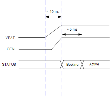
Cut off the power supply of VBAT, the module will automatically execute turn-off procedure.
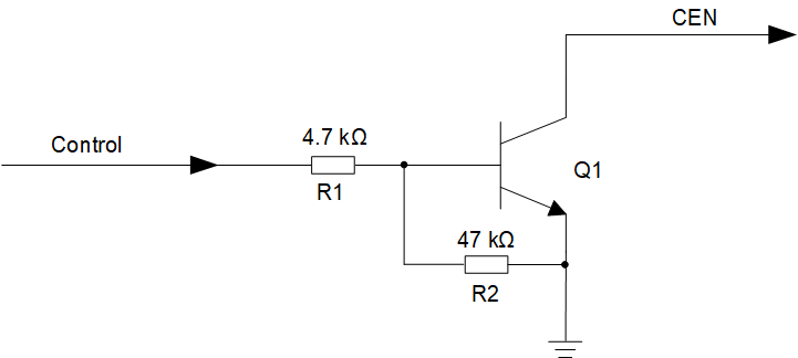
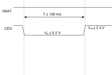
Reset
Drive CEN low for at least 100 ms and then release it to reset the module.
Pin Definition of Reset Pin:
| Pin Name | Pin No. | Description | Comment |
|---|---|---|---|
| CEN | 9 | Resets the module | Internally pulled up to 3.3 V. Hardware reset; active low |
The reference designs for resetting the module are shown below. An open collector driving circuit or a button can be used to control the CEN pin.
The reset timing is illustrated in the following figure.
Wireless Application Interfaces
UARTs
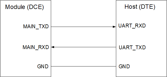
The module provides two UARTs: the main UART and the debug UART. The module is used as DCE (Data Communication Equipment), and is connected in the traditional DCE-DTE (Data Terminal Equipment) mode.
Pin Definition of UARTs:
| Pin Name | Pin No. | I/O | Description | Comment |
|---|---|---|---|---|
| MAIN_TXD | 20 | DO | Main UART transmits | |
| MAIN_RXD | 19 | DI | Main UART receives | |
| DBG_TXD | 26 | DO | Debug UART transmits | Test points must be reserved. |
| DBG_RXD | 25 | DI | Debug UART receives |
The main UART can be used for AT command communication and data transmission. The default baud rate is 115200 bps, and the maximum baud rate can reach 2 Mbps.
The main UART is also available for firmware upgrade and supports a default baud rate of 921600 bps.
The following is the schematic diagram of the main UART connection between DCE and DTE.
The debug UART supports 115200 bps baud rate by default, and is used for the output of partial logs.
The following is a reference design of debug UART.
SPI*
FC41D provides a SPI that supports both master and slave modes. The maximum clock frequency of the interface can reach 50 MHz in slave mode, and 8 MHz in the master mode.
The pin description of SPI is shown as below:
Pin Definition of SPI:
| Pin Name | Pin No. | I/O | Description | Comment |
|---|---|---|---|---|
| SPI_MISO | 13 | DIO | SPI master input slave output | |
| SPI_MOSI | 14 | DIO | SPI master output slave input | |
| SPI_CLK | 17 | DIO | SPI clock | In master mode, it's an output signal; in slavemode, it's an input signal. |
| SPI_CS | 18 | DIO | SPI chip select | In master mode, it's an input signal; in slave mode, it's an output signal. |
I2C Interface*
FC41D provides an I2C interface that supports master mode only with maximum clock frequency of 400 kHz and 7-bit addressing. It can be used to connect peripherals such as EEPROM.
Pin Definition of I2C Interface:
| Pin Name | Pin No. | I/O | Description | Comment |
|---|---|---|---|---|
| I2C_SCL | 4 | OD | I2C serial clock | Requires external pull-up to 3.3 V. |
| I2C_SDA | 5 | OD | I2C serial data | Requires external pull-up to 3.3 V. |
PWM Interface*
FC41D provides 1 PWM channel by default. The following table shows the pin description of PWM interface.
Pin Definition of PWM Interface:
| Pin Name | Pin No. | I/O | Description |
|---|---|---|---|
| PWM | 11 | DO | Pulse width modulation output channel |
WAKEUP Interface
WAKEUP_IN pin can wake up the module from deep sleep mode or standby mode, while WAKEUP_OUT pin can be used to wake up the host.
Pin Definition of WAKEUP Interface:
| Pin Name | Pin No. | I/O | Description | Comment |
|---|---|---|---|---|
| WAKEUP_IN | 7 | DI | Wakes up the module fromdeep sleep or standby mode | Rising edge wakeup. |
| WAKEUP_OUT | 8 | DO | Wakes up the host | Active high. |
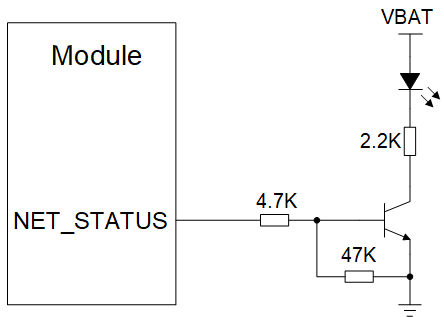
Network Status Indication
The network indication pin NET_STATUS can drive the network status indicators.
The following table describes the pin definition and logic level changes of NET_STATUS.
Pin Definition of NET_STATUS:
| Pin Name | Pin No. | I/O | Description | Comment |
|---|---|---|---|---|
| NET_STATUS | 12 | DO | Indicates the module's network activity status. | Outputs high level when Wi-Fi is connected in STA mode. |
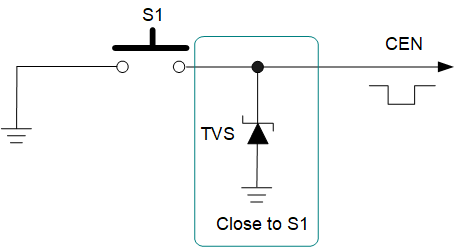
A reference circuit is shown in the following figure.
GPIO Interfaces*
FC41D provides 4 GPIO interfaces by default. The following table shows the pin description of GPIOs.
Pin Definition of GPIO Interfaces:
| Pin Name | Pin No. | I/O | Description | Comment |
|---|---|---|---|---|
| GPIO1 | 10 | DIO | General-purpose input/output | Wake-up interrupt. |
| GPIO2 | 22 | DIO | General-purpose input/output | Wake-up interrupt. |
| GPIO3 | 23 | DIO | General-purpose input/output | Wake-up interrupt. |
| GPIO4 | 24 | DIO | General-purpose input/output | Wake-up interrupt. |
ADC Interface*
The module provides one ADC interface by default, and the voltage range is 0--2.4 V. To improve the accuracy of ADC, surround the trace of ADC with ground.
Pin Definition of ADC Interface:
| Pin Name | Pin No. | I/O | Description |
|---|---|---|---|
| ADC | 21 | AI | General-purpose ADC interface |
ADC Features:
| Parameter | Min. | Typ. | Max. | Unit |
|---|---|---|---|---|
| ADC Voltage Range | 0 | - | 2.4 | V |
| ADC Resolution Rate | - | 13 | - | bit |
| ADC Sample Rate | - | 6 | - | MHz |
Antenna Interfaces
FC41D provides PCB antenna, coaxial RF connector and ANT_WIFI/BT (stamphole). The coaxial RF connector is not mounted on the module when using PCB antenna or ANT_WIFI/BT. FC41D supports PCB antenna by default;coaxial RF connector and ANT_WIFI/BT are optional.
Operating Frequencies
The operating frequencies of FC41D is shown in the table below:
Operating Frequencies (Unit: GHz):
| Mode | Frequency |
|---|---|
| 2.4 GHz Wi-Fi | 2.412--2.484 |
| Bluetooth | 2.402--2.480 |
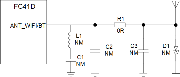
ANT_WIFI/BT Antenna(Optional)
ANT_WIFI/BT pin description is as below:
Antenna Pin Definition:
| Pin Name | Pin No. | I/O | Description | Comment |
|---|---|---|---|---|
| ANT_WIFI/BT | 2 | AIO | Wi-Fi/Bluetooth antenna interface | 50 Ω impedance. |
The circuit of RF antenna interface is shown below. In order to achieve better RF performance, it is necessary to reserve LC and π matching circuit. Matching components such as R1, L1, C1, C2, C3 and D1 should be placed as close to the antenna as possible, L1, C1, C2, C3 and D1 are not mounted by default. The parasitic capacitance of TVS should be less than 0.05 pF.
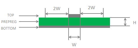
RF Routing Guidelines
For user's PCB, the characteristic impedance of all RF traces should be controlled to 50 Ω. The impedance of the RF traces is usually determined by the trace width (W), the materials' dielectric constant, the height from the reference ground to the signal layer (H), and the spacing between RF traces and grounds (S). Microstrip or coplanar waveguide is typically used in RF layout to control characteristic impedance. The following are reference designs of microstrip or coplanar waveguide with different PCB structures.
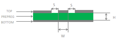
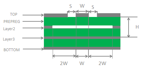
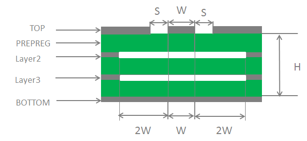
To ensure RF performance and reliability, follow the principles below in RF layout design:
- Use an impedance simulation tool to accurately control the
characteristic impedance of RF traces to 50 Ω. - The GND pins adjacent to RF pins should not be designed as thermal relief pads, and should be fully connected to ground.
- The distance between the RF pins and the RF connector should be as short as possible and all the right-angle traces should be changed to curved ones. The recommended trace angle is 135°.
- There should be clearance under the signal pin of the antenna connector or solder joint.
- The reference ground of RF traces should be complete. Meanwhile,adding some ground vias around RF traces and the reference ground could help to improve RF performance. The distance between the ground vias and RF traces should be not less than twice the width of RF signal traces (2 × W).
- Keep RF traces away from interference sources, and avoid intersection and paralleling between traces on adjacent layers.
For more details about RF layout, see document [2].
Antenna Design Requirements
Antenna Design Requirements:
| Type | Requirement |
|---|---|
| Frequency Ranges (GHz) | 2.4 GHz Wi-Fi: 2.412--2.484 Bluetooth: 2.402--2.480 |
| Cable Insertion Loss(dB) | < 1 |
| VSWR | ≤ 2 |
| Gain (dBi) | 1 (Typ.) |
| Max. input power (W) | 50 |
| Input impedance (Ω) | 50 |
| Polarization type | Vertical |
RF Connector Recommendation
If RF connector is used for antenna connection, it is recommended to use the U.FL-R-SMT connector provided by Hirose.
U.FL-LP series mated plugs listed in the following figure can be used to match the U.FL-R-SMT connector.
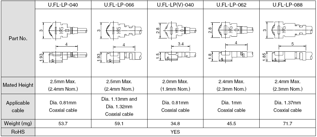
The following figure describes the space factor of mated connectors.
For more details, please visithttp://www.hirose.com.
On Board PCB Antenna
On Board PCB Antenna Characteristics:
| Parameter | Min. | Typ. | Max. | Unit |
|---|---|---|---|---|
| Frequency | 2400 | - | 2500 | MHz |
| Impedance | - | 50 | - | Ω |
| VSWR | - | - | 3 | - |
| Gain | - | -1.81 | - | dBi |
| Efficiency | - | 35 % | - | - |
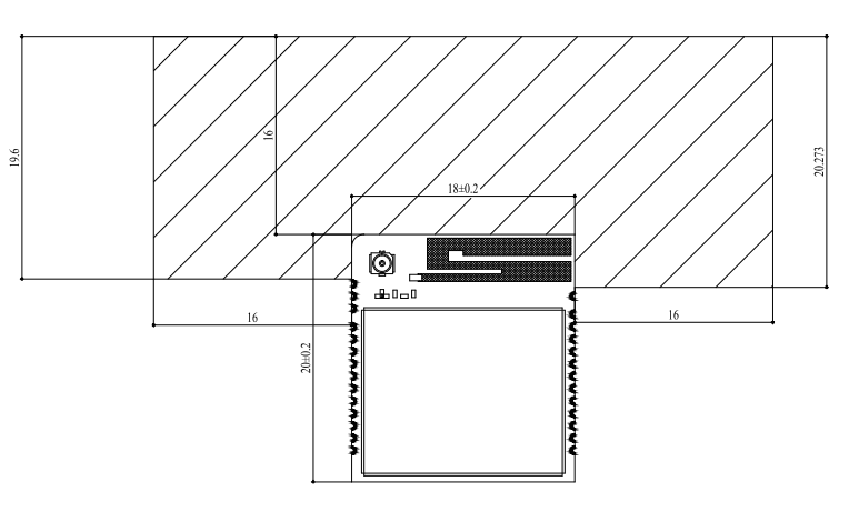
When using the PCB antenna on the module, the module should be placed on the side of the motherboard. The distance between the PCB antenna and connectors, vias, traces, copper area and any other metal components on the motherboard should be at least 16 mm. All layers in the PCB of the motherboard under the PCB antenna should be designed as a keepout area.
Coaxial RF Connector (Optional)
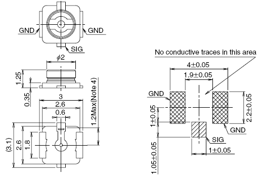
Receptacle Specifications
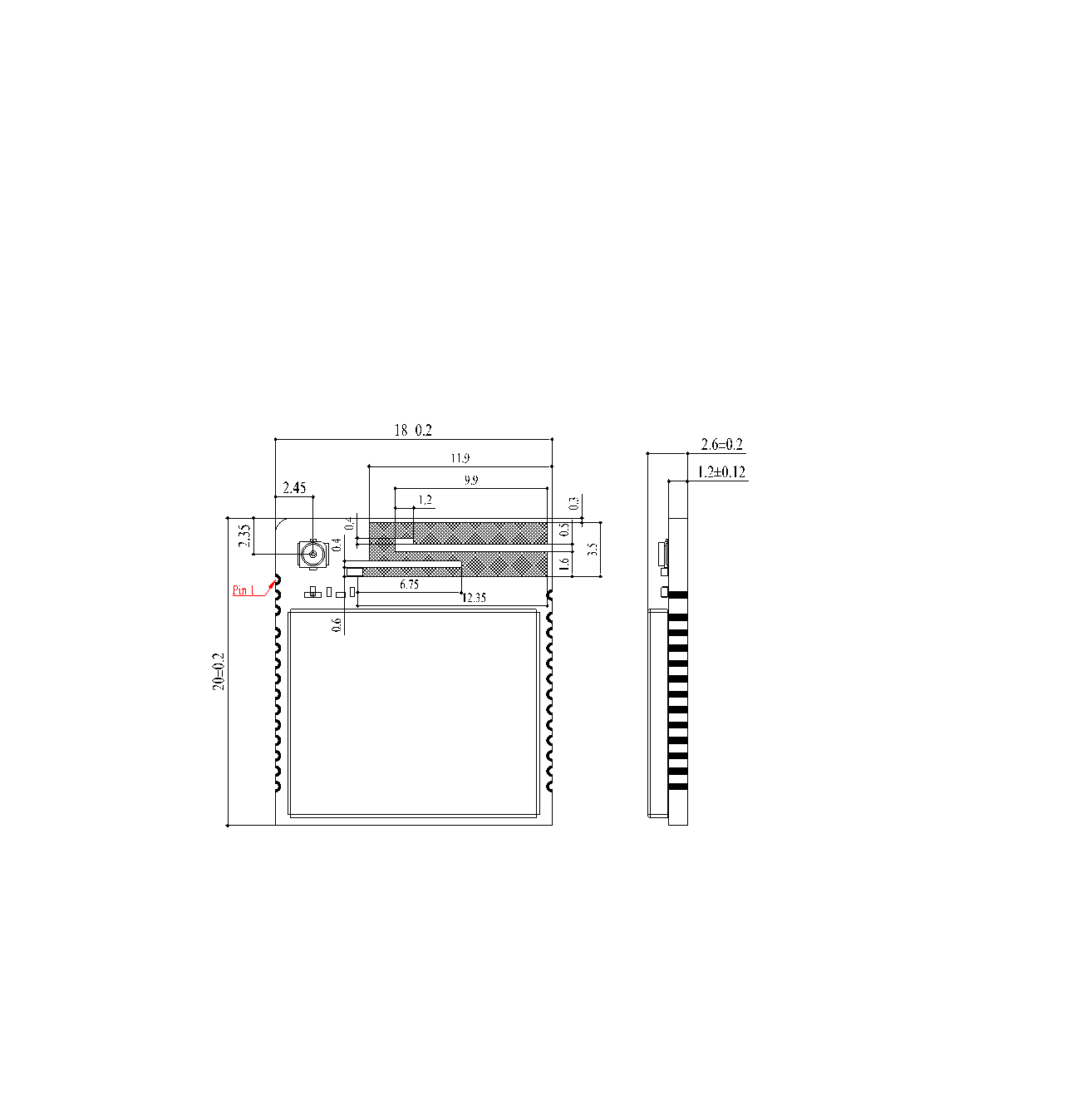
The mechanical dimensions of the receptacle provided by the module are as follows.
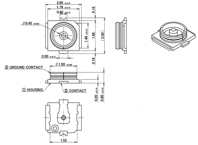
Major Specifications of the RF Connector:
| Item | Specification |
|---|---|
| Nominal Frequency Range | DC to 6 GHz |
| Nominal Impedance | 50 Ω |
| Temperature Rating | -40 °C to +85 °C |
| Voltage Standing Wave Ratio(VSWR) | Meet the requirements of: Max. 1.3 (DC--3 GHz) Max. 1.45 (3--6 GHz) |
Antenna Connector Installation
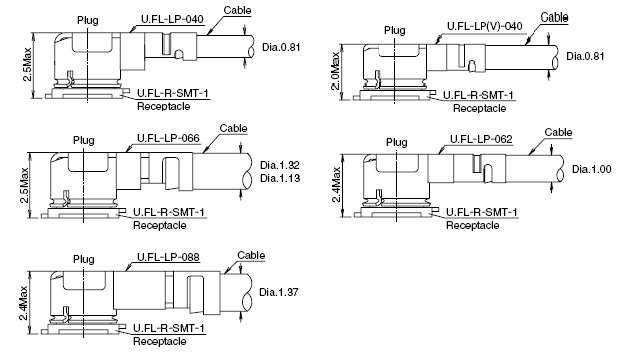
The receptacle mounted on the module accepts two types of mated plugs that will meet a maximum height of 1.2 mm using a Ø 0.81 mm coaxial cable or a maximum height of 1.45 mm utilizing a Ø 1.13 mm coaxial cable.
The following figure shows the dimensions of mated plugs using Ø 0.81 mm coaxial cables.
The following figure illustrates the connection between the receptacle on FC41D and the mated plug using a Ø 0.81 mm coaxial cable.
The following figure illustrates the connection between the receptacle on FC41D and the mated plug using a Ø 1.13 mm coaxial cable.
Assemble Coaxial Cable Plug Manually
The pictures for plugging in a coaxial cable plug is shown below, θ =90° is acceptable, while θ ≠ 90° is not.
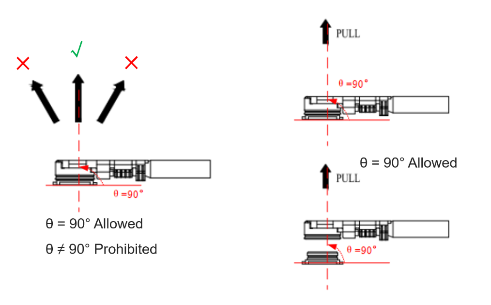
The pictures of pulling out the coaxial cable plug is shown below, θ =90° is acceptable, while θ ≠ 90° is not.
Assemble Coaxial Cable Plug with Jig
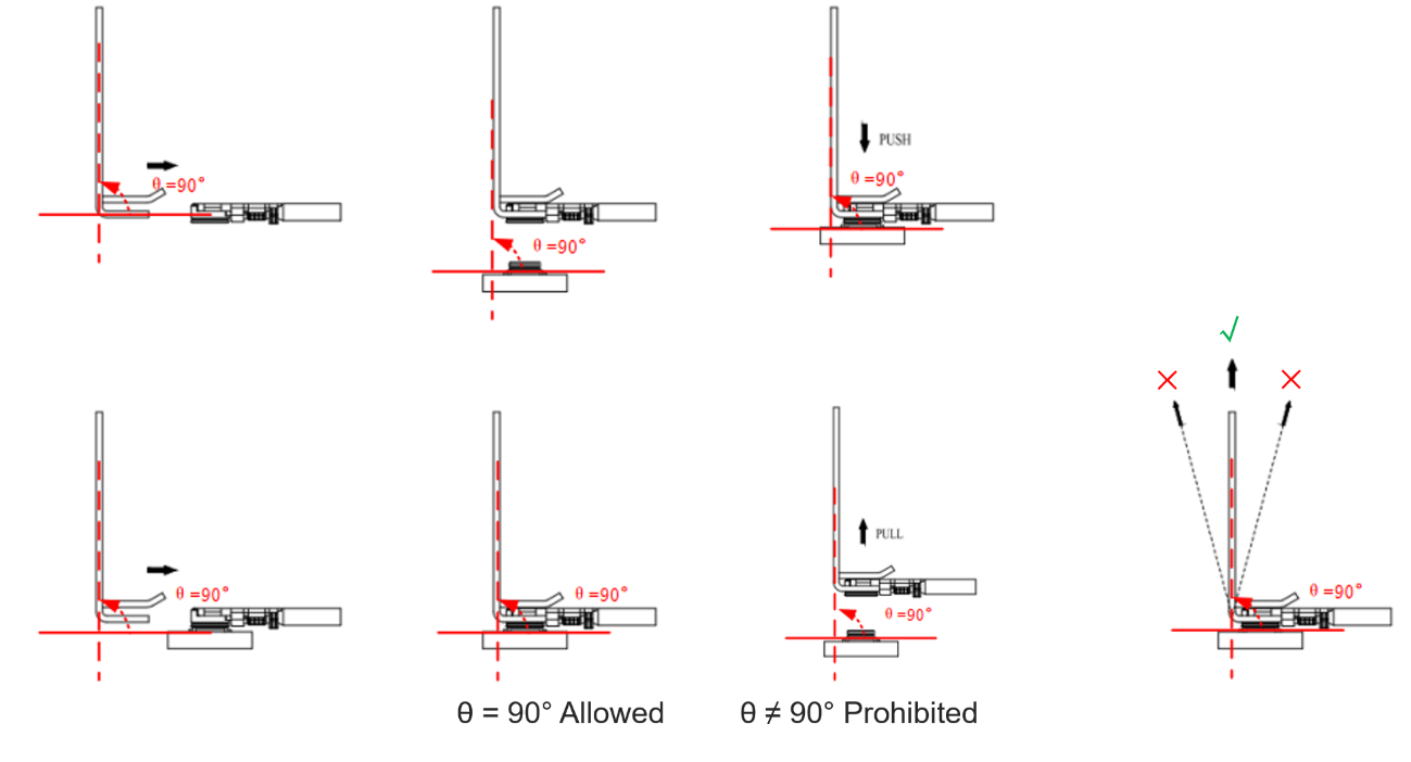
The pictures of installing the coaxial cable plug with a jig is shown below, θ = 90° is acceptable, while θ ≠ 90° is not.
Recommended Manufacturers of RF Connector and Cable
RF connectors and cables by I-PEX are recommended. For more details,visit https://www.i-pex.com.
Reliability, Radio and Electrical Characteristics
Absolute Maximum Ratings
Absolute maximum ratings for power supply and voltage on digital and analog pins of the module are listed in the following table.
Absolute Maximum Ratings:
| Parameter | Min. | Max. | Unit |
|---|---|---|---|
| VBAT | -0.3 | 3.9 | V |
| I/O input voltage | -0.3 | 3.9 | V |
Power Supply Ratings
Module Power Supply Ratings:
| Parameter | Min. | Typ. | Max. | Unit |
|---|---|---|---|---|
| VBAT | 3.0 | 3.3 | 3.6 | V |
Digital I/O Characteristics
Digital I/O Requirements:
| Parameter | Min. | Typ. | Max. | Unit |
|---|---|---|---|---|
| VIH | High-level Input Voltage | 0.7 ×VBAT | VBAT + 0.2 | V |
| VIL | Low-level Input Voltage | -0.3 | 0.3 ×VBAT | V |
| VOH | High-level Output Voltage | 0.9 ×VBAT | VBAT | V |
| VOL | Low-level Output Voltage | 0 | 0.1 ×VBAT | V |
| IiL | Input Leakage Current | -5 | 5 | µA |
Power Consumption
Power Consumption in Low Power Modes
Power Consumption in Low Power Modes:
| Parameter | Description | Typ. | Unit |
|---|---|---|---|
| Deep sleep mode | AT+QDEEPSLEEP can set the module to deep sleep mode.In this case, the UARTs stop working and software settings are not saved. | 8.6 | μA |
| Standby mode | AT+QLOWPOWER can set the module to standby mode.In this case, the UARTs stop working but software settings can be saved. | 30 | μA |
| Idle state | Neither Wi-Fi nor Bluetooth does any operation. | 22.74 | mA |
NOTE:
For more information about AT command, please refer to document [4].
Power Consumption in Normal Operating Modes
Power Consumption in Normal Operating Modes:
| Parameter | Description | Typ. | Unit |
|---|---|---|---|
| Wi-Fi Scan | Scan in every 2 s | 68.59 | mA |
| Wi-Fi Connected | STA mode is ON, but no STA device is connected | 74.52 | mA |
| Wi-Fi Connected | SoftAP mode is ON, and 1 STA device is connected | 77.11 | mA |
| Wi-Fi Connected | SoftAP mode is ON, and 2 STA devices are connected | 77.29 | mA |
| Wi-Fi Connected | SoftAP mode is ON, but no STA device is connected | 77.09 | mA |
| Data Transmission | SoftAP mode data transmission | 155.29 | mA |
| Data Transmission | STA mode data transmission | 147.81 | mA |
| Data Transmission | SoftAP mode + BLE Server mode data transmission | 157.56 | mA |
| Data Transmission | STA mode + BLE Server mode data transmission | 149.66 | mA |
| Bluetooth Connected | Receives data as Server | 28.41 | mA |
| Bluetooth Connected | Transmits data as Server | 28.39 | mA |
| Bluetooth Connected | Receives data as Client | 23.68 | mA |
| Bluetooth Connected | Transmits data as Client | 23.68 | mA |
| RF Non-signaling Mode | 802.11b Tx (2.4 GHz) @ 1 Mbps | 91 | mA |
| RF Non-signaling Mode | 802.11b Tx (2.4 GHz) @ 11 Mbps | 92 | mA |
| RF Non-signaling Mode | 802.11g Tx (2.4 GHz) @ 6 Mbps | 90 | mA |
| RF Non-signaling Mode | 802.11g Tx (2.4 GHz) @ 54 Mbps | 88 | mA |
| RF Non-signaling Mode | 802.11n Tx (2.4 GHz) @ HT20 MCS0 | 89 | mA |
| RF Non-signaling Mode | 802.11n Tx (2.4 GHz) @ HT20 MCS7 | 88 | mA |
RF Performances
Wi-Fi Performances
2.4 GHz Wi-Fi Conducted Output Power:
| Protocol | Rate | Min. (dBm) | Typ. (dBm) |
|---|---|---|---|
| 802.11b | 1 Mbps | 14 | 16 |
| 802.11b | 11 Mbps | 14 | 16 |
| 802.11g | 6 Mbps | 13 | 15 |
| 802.11g | 54 Mbps | 12 | 14 |
| 802.11n, HT20 | MCS 0 | 12 | 14 |
| 802.11n, HT20 | MCS 7 | 11 | 13 |
2.4 GHz Wi-Fi Conducted Receiving Sensitivity:
| Protocol | Rate | Typ. (dBm) |
|---|---|---|
| 802.11b | 1 Mbps | -96 |
| 802.11b | 11 Mbps | -87 |
| 802.11g | 6 Mbps | -91 |
| 802.11g | 54 Mbps | -74 |
| 802.11n, HT20 | MCS 0 | -90 |
| 802.11n, HT20 | MCS 7 | -71 |
2.4 GHz Wi-Fi OTA TRP Test:
| Protocol | Rate | Typ. (dBm) |
|---|---|---|
| 802.11b | 1 Mbps | 15 |
| 802.11b | 11 Mbps | 15 |
| 802.11g | 6 Mbps | 14 |
| 802.11g | 54 Mbps | 13 |
| 802.11n, HT20 | MCS 0 | 13 |
| 802.11n, HT20 | MCS 7 | 12 |
2.4 GHz Wi-Fi OTA TIS Test:
| Protocol | Rate | Typ. (dBm) |
|---|---|---|
| 802.11b | 1 Mbps | -94 |
| 802.11b | 11 Mbps | -85 |
| 802.11g | 6 Mbps | -88 |
| 802.11g | 54 Mbps | -71 |
| 802.11n, HT20 | MCS 0 | -86 |
| 802.11n, HT20 | MCS 7 | -66 |
BLE Performances
BLE Conducted Output Power / Receiving Sensitivity:
| Operating Mode | Output Power (Typ.) | Receiving Sensitivity (Typ.) | Unit |
|---|---|---|---|
| BLE (1 Mbps) | 6 | -95 | dBm |
ESD Protection
Static electricity occurs naturally and it may damage the module.Therefore, applying proper ESD countermeasures and handling methods is imperative. For example, wear anti-static gloves during the development,production, assembly and testing of the module; add ESD protection components to the ESD sensitive interfaces and points in the product design.
ESD Characteristics (Temperature: 25–30 ºC, Humidity: 40 ±5 %):
| Tested Interfaces | Contact Discharge | Air Discharge | Unit |
|---|---|---|---|
| VBAT, GND | ±4 | ±8 | kV |
| ANT_WIFI/BT | ±4 | ±8 | kV |
| Other Interfaces | ±0.5 | ±1 | kV |
Operating and Storage Temperatures
Operating and Storage Temperatures (Unit: ºC):
| Parameter | Min. | Typ. | Max. |
|---|---|---|---|
| Operating Temperature Range2 | -40 | +25 | +85 |
| Storage Temperature Range | -45 | - | +95 |
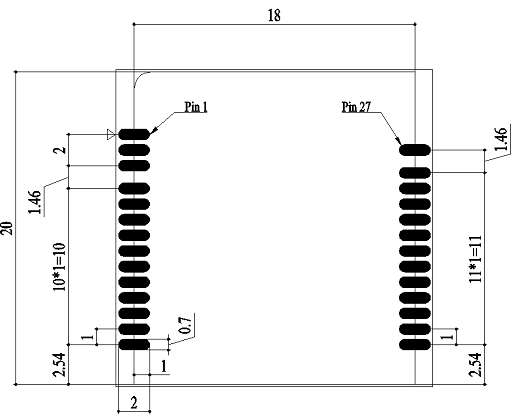
Mechanical Information
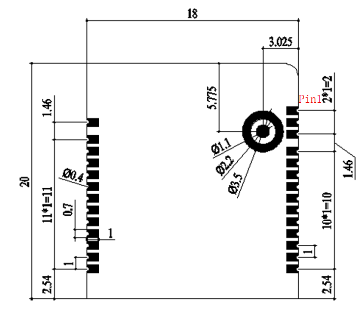
This chapter describes the mechanical dimensions of the module. All dimensions are measured in millimeter (mm), and the dimensional tolerances are ±0.2 mm unless otherwise specified.
Mechanical Dimensions
NOTE:
The package warpage level of the module conforms to the JEITA ED-7306 standard.
Recommended Footprint
NOTE:
Keep at least 3 mm between the module and other components on the motherboard to improve soldering quality and maintenance convenience.
Top and Bottom Views
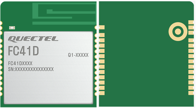
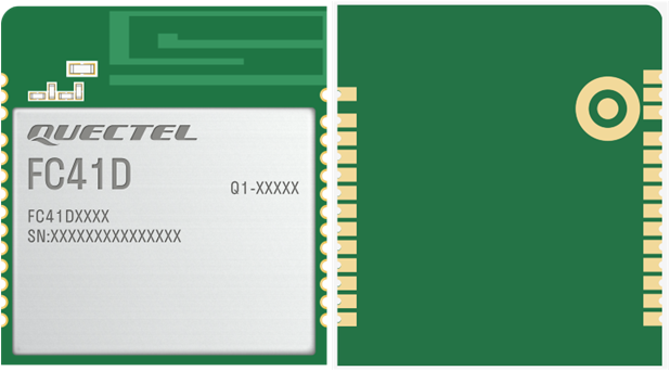
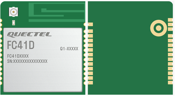
NOTE:
Images above are for illustration purpose only and may differ from the actual module. For authentic appearance and label, please refer to the module received from Quectel.
Storage, Manufacturing & Packaging
Storage Conditions
The module is provided with vacuum-sealed packaging. MSL of the module
is rated as 3. The storage requirements are shown below.
- Recommended Storage Condition: the temperature should be 23 ±5 °C and the relative humidity should be 35--60 %.
- Shelf life (in a vacuum-sealed packaging): 12 months in Recommended Storage Condition.
- Floor life: 168 hours 3 in a factory where the temperature is 23 ±5 °C and relative humidity is below 60 %. After the vacuum-sealed packaging is removed, the module must be processed in reflow soldering or other high-temperature operations within 168 hours.Otherwise, the module should be stored in an environment where the relative humidity is less than 10 % (e.g., a dry cabinet).
- The module should be pre-baked to avoid blistering, cracks and inner-layer separation in PCB under the following circumstances:
- The module is not stored in Recommended Storage Condition;
- Violation of the third requirement mentioned above;
- Vacuum-sealed packaging is broken, or the packaging has been removed for over 24 hours;
- Before module repairing.
- If needed, the pre-baking should follow the requirements below:
- The module should be baked for 8 hours at 120 ±5 °C;
- The module must be soldered to PCB within 24 hours after the baking,otherwise it should be put in a dry environment such as in a dry cabinet.
NOTE:
- To avoid blistering, layer separation and other soldering issues, extended exposure of the module to the air is forbidden.
- Take out the module from the package and put it on high-temperature-resistant fixtures before baking. If shorter baking time is desired, see IPC/JEDEC J-STD-033 for the baking procedure.
- Pay attention to ESD protection, such as wearing anti-staticgloves, when touching the modules.
Manufacturing and Soldering
Push the squeegee to apply the solder paste on the surface of stencil,thus making the paste fill the stencil openings and then penetrate to the PCB. Apply proper force on the squeegee to produce a clean stencil surface on a single pass. To guarantee module soldering quality, the thickness of stencil for the module is recommended to be 0.15--0.18 mm.For more details, see document [3].
The recommended peak reflow temperature should be 235--246 ºC, with 246ºC as the absolute maximum reflow temperature. To avoid damage to the module caused by repeated heating, it is recommended that the module should be mounted only after reflow soldering for the other side of PCB has been completed. The recommended reflow soldering thermal profile (lead-free reflow soldering) and related parameters are shown below.
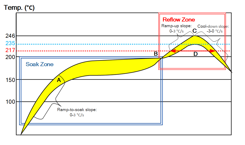
Recommended Thermal Profile Parameters:
| Factor | Recommended Value |
|---|---|
| Soak Zone | |
| Ramp-to-soak slope | 0--3 °C/s |
| Soak time (between A and B: 150 °C and 200 °C) | 70--120 s |
| Reflow Zone | |
| Ramp-up slope | 0--3 °C/s |
| Reflow time (D: over 217 °C) | 40--70 s |
| Max. temperature | 235--246 °C |
| Cool-down slope | -3--0 °C/s |
| Reflow Cycle | |
| Max. reflow cycle | 1 |
NOTE:
- The above profile parameter requirements are for the measured temperature of the solder joints. Both the hottest and coldestspots of solder joints on the PCB should meet theaboverequirements.
- During manufacturing and soldering, or any other processes that may contact the module directly, NEVER wipe the module's shielding can with organic solvents, such as acetone, ethyl alcohol, isopropyl alcohol, trichloroethylene, etc. Otherwise,the shielding can may become rusted.
- The shielding can for the module is made of Cupro-Nickel base material. It is tested that after 12 hours' Neutral Salt Spraytest, the laser engraved label information on the shielding can is still clearly identifiable and the QR code is still readable,although white rust may be found.
- If a conformal coating is necessary for the module, do NOT use any coating material that may chemically react with the PCB or shielding cover, and prevent the coating material from flowing into the module.
- Avoid using ultrasonic technology for module cleaning since it can damage crystals inside the module.
- Due to the complexity of the SMT process, please contact Quectel Technical Support in advance for any situation that you are notsure about, or any process (e.g. selective soldering, ultrasonic soldering) that is not mentioned in document [3].
Packaging Specifications
This chapter describes only the key parameters and process of packaging.All figures below are for reference only. The appearance and structure of the packaging materials are subject to the actual delivery.
The module adopts carrier tape packaging and details are as follow:
Carrier Tape
Dimension details are as follow:
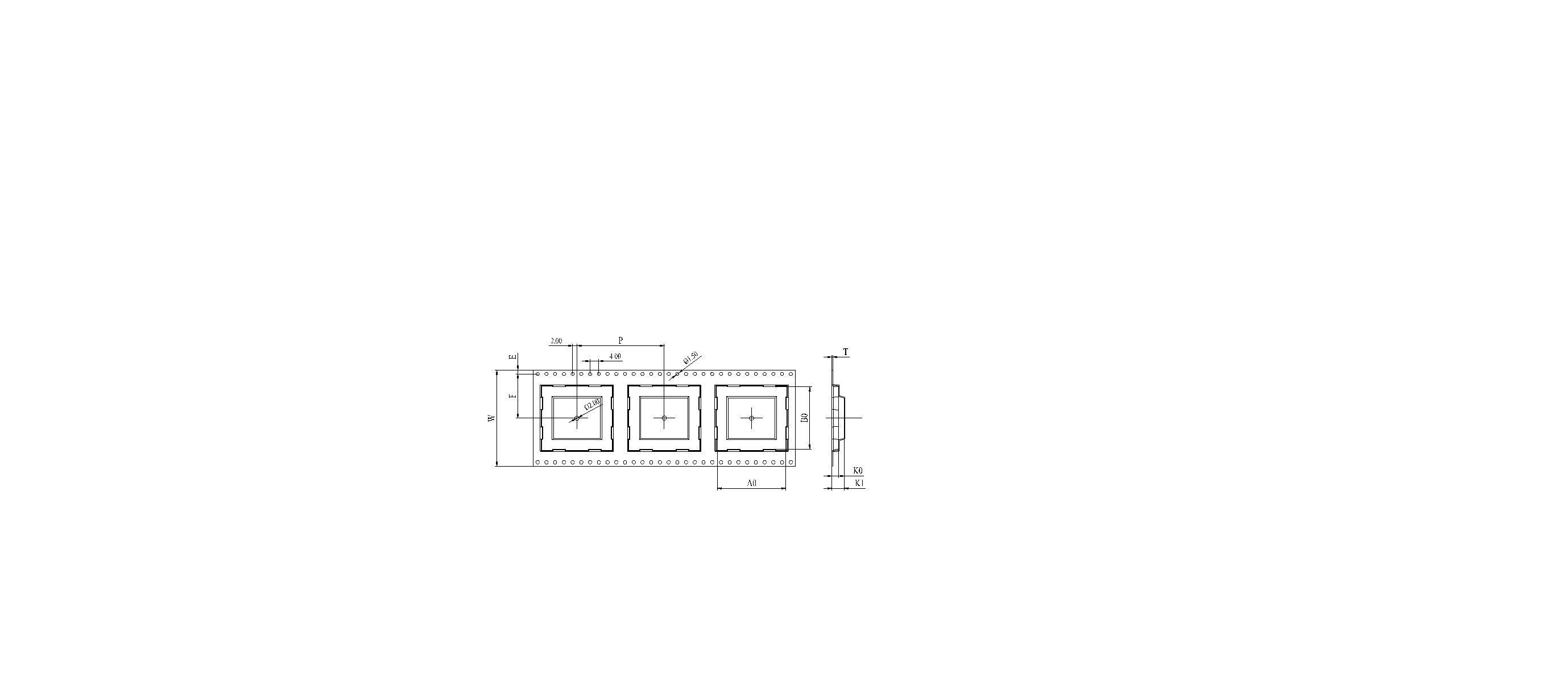
Carrier Tape Dimension Table (Unit: mm):
| W | P | T | A0 | B0 | K0 | K1 | F | E |
|---|---|---|---|---|---|---|---|---|
| 44 | 32 | 0.4 | 18.5 | 20.5 | 3 | 6.8 | 20.2 | 1.75 |
Plastic Reel
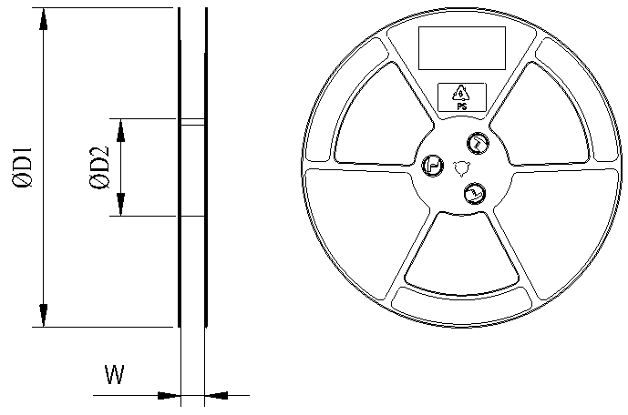
Plastic Reel Dimension Table (Unit: mm):
| øD1 | øD2 | W |
|---|---|---|
| 330 | 100 | 44.5 |
Mounting Direction
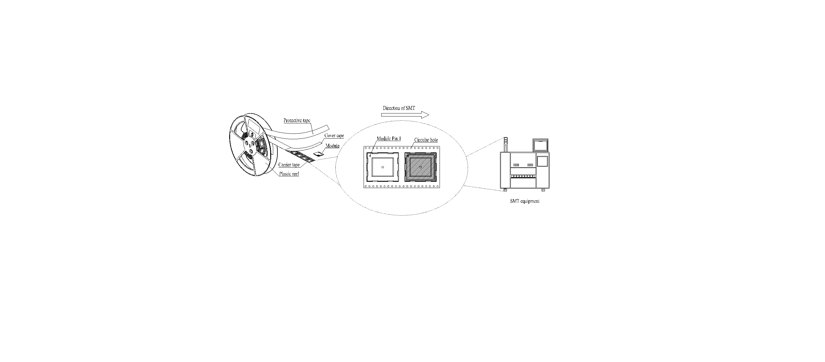
Packaging Process
Place the module into the carrier tape and use the cover tape to cover it; then wind the heat-sealed carrier tape to the plastic reel and use the protective tape for protection. 1 plastic reel can load 250 modules.
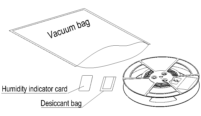
Place the packaged plastic reel, 1 humidity indicator card and 1 desiccant bag into a vacuum bag, vacuumize it.
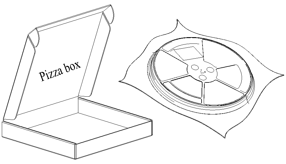
Place the vacuum-packed plastic reel into the pizza box.
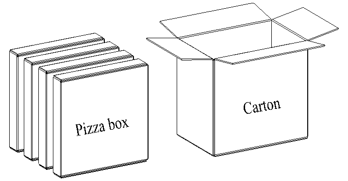
Put 4 packaged pizza boxes into 1 carton box and seal it. 1 carton box can pack 1000 modules.
Appendix References
Reference Documents:
| Document Name |
|---|
| [1] Quectel_FC41D_TE-B_User_Guide. |
| [2]Quectel_RF_Layout_Application_Note |
| [3]Quectel_Module_SMT_Application_Note |
| [4] Quectel_FC41D_AT_Commands_Manual |
Terms and Abbreviations:
| Abbreviation | Description |
|---|---|
| ADC | Analog-to-Digital Converter |
| AP | Access Point |
| ARM | Advanced RISC Machine |
| BLE | Bluetooth Low Energy |
| BPSK | Binary Phase Shift Keying |
| CCK | Complementary Code Keying |
| DCE | Data Communication Equipment |
| DTE | Data Terminal Equipment |
| EEPROM | Electrically Erasable Programmable Read-Only Memory |
| ESD | Electrostatic Discharge |
| GFSK | Gauss Frequency Shift Keying |
| GND | Ground |
| GPIO | General-Purpose Input/Output |
| HT | High Throughput |
| I2C | Inter-Integrated Circuit |
| I/O | Input/Output |
| IEEE | Institute of Electrical and Electronics Engineers |
| IiL | Input Leakage Current |
| LCC | Leadless Chip Carrier |
| Mbps | Megabits per second |
| MCS | Modulation and Coding Scheme |
| MSL | Moisture Sensitivity Level |
| OTA | Over The Air |
| PCB | Printed Circuit Board |
| PCM | Pulse Code Modulation |
| PWM | Pulse Width Modulation |
| QAM | Quadrature Amplitude Modulation |
| QPSK | Quadrature Phase Shift Keying |
| RAM | Random Access Memory |
| RF | Radio Frequency |
| RoHS | Restriction of Hazardous Substances |
| RXD | Receive Data (Pin) |
| SPI | Serial Peripheral Interface |
| STA | Station |
| TIS | Total Isotropic Sensitivity |
| TRP | Total Radiated Power |
| TVS | Transient Voltage Suppressor |
| TXD | Transmit Data (Pin) |
| UART | Universal Asynchronous Receiver/Transmitter |
| VIH | High-level Input Voltage |
| VIL | Low-level Input Voltage |
| Vnom | Normal Voltage Value |
| VOH | High-level Output Voltage |
| VOL | Low-level Output Voltage |
| VSWR | Voltage Standing Wave Ratio |
Within the operating temperature range, the module's related performance meets IEEE and Bluetooth specifications.↩
Within the operating temperature range, the module's related performance meets IEEE and Bluetooth specifications.↩
This floor life is only applicable when the environment conform to IPC/JEDEC J-STD-033. It is recommended to start the solder reflow process within 24 hours after the package is removed if the temperature and moisture do not conform to, or are not sure to conform to IPC/JEDEC J-STD-033. Do not unpack the modules in large quantities until they are ready for soldering.↩