

 English
HCM511S Hardware Design
Introduction
This document defines HCM511S in GSDK solution and describes its hardware interfaces and air interfaces, which are connected with your applications. The document provides a quick insight into interface specifications, RF performance, electrical and mechanical specifications, as well as other related information of the module.
Product Overview
HCM511S is a low-power and high performance MCU Bluetooth module supporting BLE 5.4 protocol. It integrates a highly configurable wireless transceiver. The module also provides multiple interfaces such as USART, EUART, SWD, I2C, ADC and PDM for various applications.
It is an SMD module with compact packaging. The general features of the module are as follows:
- Embedded 32-bit ARM Cortex-M33 processor with a frequency of up to 76.8 MHz
- 32 KB RAM and 352 KB/ 512 KB flash 1
- Flexible and efficient power consumption management
- Bluetooth mesh network low-power nodes 2
- Support for Peripheral Reflex System (PRS) for autonomous inter-peripheral signaling
- Support for OTA (Over-The-Air Upgrade)
- Support for secondary development
Basic Information:
| HCM511S | |
|---|---|
| Packaging type | LCC |
| Pin counts | 24 |
| Dimensions | (16.6 +0.3/-0.15) mm × (11.2 +0.3/-0.15) mm ×(2.1 ±0.2) mm |
| Weight | Approx. 0.57 g |
Key Features
Key Features:
| Basic Information | |
|---|---|
| Protocol and Standard | |
| Power Supply | VBAT Power Supply: |
| Temperature Ranges | |
| TE-B Kit | HCM511S-TE-B 4 |
| Antenna | |
| Antenna | |
| Application Interface 5 | |
| Application Interfaces | USART, EUART, SWD, I2C, ADC, PDM, GPIO |
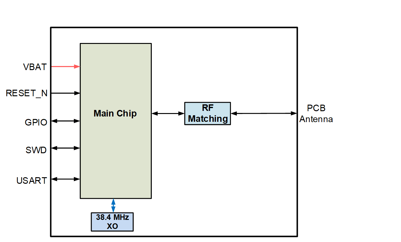
Functional Diagram
NOTE:
The module supports 1 USART, 1 SWD and 14 GPIO interfaces by default.In the case of multiplexing, it supports interfaces including EUART,I2C, ADC and PDM. For more details, see Chapter 3.3 and Chapter 3.4.
Application Interfaces
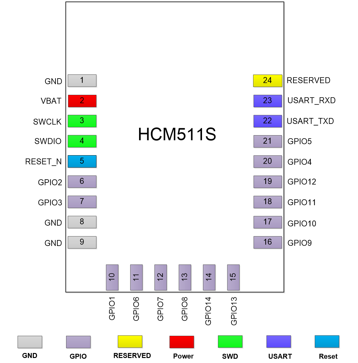
Pin Assignment
NOTE:
- Keep the RESERVED and all unused pins unconnected.
- All GND pins should be connected to ground.
- The module supports 1 USART, 1 SWD and 14 GPIO interfaces by default. In the case of multiplexing, it supports interfaces including EUART, I2C, ADC and PDM. For more details, see Chapter 3.3 and Chapter 3.4.
Pin Descriptions
Parameter Description:
| Parameter | Description |
|---|---|
| DI | Digital Input |
| DO | Digital Output |
| DIO | Digital Input/Output |
| PI | Power Input |
DC characteristics include power domain and rated current.
Pin Description:
Power Supply and GND Pins:
| Pin Name | Pin No. | I/O | Description | DC Characteristics | Comment |
|---|---|---|---|---|---|
| VBAT | 2 | PI | Power supply for the module | Vmax = 3.8 V Vmin = 1.71 V Vnom = 3.3 V |
It must be provided with sufficient current more than 20 mA. |
| GND | 1, 3, 30, 31--39 |
Reset:
| Pin Name | Pin No. | I/O | Description | DC Characteristics | Comment |
|---|---|---|---|---|---|
| RESET_N | 5 | DI | Reset the module | 1.8 V | Hardware reset. Internally pulled up to 1.8 V Active low. |
USART:
| Pin Name | Pin No. | I/O | Description | DC Characteristics | Comment |
|---|---|---|---|---|---|
| USART_TXD | 22 | DO | USART transmit | VBAT | Used for debugging. |
| USART_RXD | 23 | DI | USART receive | VBAT | Used for debugging. |
SWD Interface:
| Pin Name | Pin No. | I/O | Description | DC Characteristics | Comment |
|---|---|---|---|---|---|
| SWDIO | 4 | DIO | Serial wire debugging input/output | VBAT | Used for program downloading. Enabled after power-up. Internally pulled up to 3.3 V. |
| SWCLK | 3 | DI | Serial wire debugging clock | VBAT | Used for program downloading. Enabled after power-up. Internally pulled down to GND. |
GPIO Interfaces:
| Pin Name | Pin No. | I/O | Description | DC Characteristics | Comment |
|---|---|---|---|---|---|
| GPIO4 | 20 | DI | Sleep wake-up control 6 | VBAT | All GPIO pins are selectable as interrupts in EM0 and EM1 mode. |
| GPIO5 | 21 | DO | Message notificationindication 7 | VBAT | All GPIO pins are selectable as interrupts in EM0 and EM1 mode. |
| GPIO1 | 10 | DIO | General-purpose input/output | VBAT | All GPIO pins are selectable as interrupts in EM0 and EM1 mode. |
| GPIO2 | 6 | DIO | General-purpose input/output | VBAT | All GPIO pins are selectable as interrupts in EM0 and EM1 mode. |
| GPIO3 | 7 | DIO | General-purpose input/output | VBAT | All GPIO pins are selectable as interrupts in EM0 and EM1 mode. |
| GPIO4 | 20 | DIO | General-purpose input/output | VBAT | All GPIO pins are selectable as interrupts in EM0 and EM1 mode. |
| GPIO5 | 21 | DIO | General-purpose input/output | VBAT | All GPIO pins are selectable as interrupts in EM0 and EM1 mode. |
| GPIO6 | 11 | DIO | General-purpose input/output | VBAT | All GPIO pins are selectable as interrupts in EM0 and EM1 mode. |
| GPIO7 | 12 | DIO | General-purpose input/output | VBAT | All GPIO pins are selectable as interrupts in EM0 and EM1 mode. |
| GPIO8 | 13 | DIO | General-purpose input/output | VBAT | All GPIO pins are selectable as interrupts in EM0 and EM1 mode. |
| GPIO10 | 17 | DIO | General-purpose input/output | VBAT | All GPIO pins are selectable as interrupts in EM0 and EM1 mode. |
| GPIO11 | 18 | DIO | General-purpose input/output | VBAT | All GPIO pins are selectable as interrupts in EM0 and EM1 mode. |
| GPIO12 | 19 | DIO | General-purpose input/output | VBAT | All GPIO pins are selectable as interrupts in EM0 and EM1 mode. |
| GPIO13 | 15 | DIO | General-purpose input/output | VBAT | All GPIO pins are selectable as interrupts in EM0 and EM1 mode. |
| GPIO14 | 14 | DIO | General-purpose input/output | VBAT | All GPIO pins are selectable as interrupts in EM0 and EM1 mode. |
Reserved Pin:
| Pin Name | Pin No. | Comment |
|---|---|---|
| RESERVED | 24 | Keep it unconnected. |
NOTE:
EM0 mode is the normal operating mode (Active mode); EM1 is the sleep mode.
GPIO Multiplexing
The module provides 14 GPIO interfaces by default, and can support up to 18 GPIO interfaces in the case of multiplexing. Pins are defined as follows:
GPIO Multiplexing (Digital Pins):
| Multiplexing Function | GPIO Interface | |||
| SWCLK, SWDIO, GPIO1–5 | GPIO6–8 | USART_TXD, USART_RXD, GPIO9–12 | GPIO13, GPIO1 | |
| EUART0_CTS | √ | √ | √ | √ |
| EUART0_RTS | √ | √ | √ | √ |
| EUART0_RXD | √ | √ | √ | √ |
| EUART0_TXD | √ | √ | √ | √ |
| I2C0_SCL | √ | √ | √ | √ | I2C0_SDA | √ | √ | √ | √ | I2C1_SCL | - | - | √ | √ |
| I2C1_SDA | - | - | √ | √ |
| PDM_CLK | √ | √ | √ | √ | PDM_DATA0 | √ | √ | √ | √ | PDM_DATA1 | √ | √ | √ | √ | USART0_CLK | √ | √ | √ | √ | USART0_CS | √ | √ | √ | √ | USART0_CTS | √ | √ | √ | √ | USART0_RTS | √ | √ | √ | √ | USART0_RXD | √ | √ | √ | √ | USART0_TXD | √ | √ | √ | √ | USART1_CLK | √ | √ | - | - | USART1_CS | √ | √ | - | - | USART1_CTS | √ | √ | - | - | USART1_RTS | √ | √ | - | - | USART1_RXD | √ | √ | - | - | USART1_TXD | √ | √ | - | - |
GPIO Multiplexing (Analog Pins):
| Multiplexing Function | SWCLK, SWDIO, GPIO1–5 | GPIO6–8 | USART_TXD,USART_RXD, GPIO9–12 | GPIO13, GPIO14 |
|---|---|---|---|---|
| ADC0 | √ | √ | √ | √ |
NOTE:
- All GPIO pins are selectable as interrupts in EM0 and EM1 modes.
- SWCLK, SWDIO, GPIO1--5, GPIO6--8 pins are selectable as interrupts in EM2 and EM3 modes.
- GPIO4, GPIO12, GPIO7, USART_TXD are available for wake-up function in EM4 mode.
- EM2 is deep sleep mode, EM3 is standby mode, and EM4 is shutoff mode.
- After the module is powered off, all of its GPlOs must be driven low. Otherwise, the current leakage may make the module enter an abnormal state.
- The maximum number of application interfaces multiplexed through GPIOs isn't available simultaneously. For the maximum number of different application interfaces that the module can support, see Chapter 3.4.
Application Interfaces
USART
The module supports 1 UASRT by default. In the case of multiplexing, it provides up to 2 USARTs. See Table 5 for more details. The USART interface supports the following applications:
- UART (supporting full-duplex communication and hardware flow control)
- RS-485
- SPI
- MicroWire
- 3-wire
- ISO 7816 Smart-Cards
- IrDA
- I2S
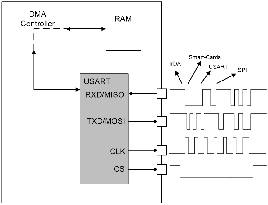
The USART operates in either asynchronous or synchronous mode:
- In synchronous mode, a separate clock signal generated by the bus master is transmitted with the data. Both the master and slave transmit data according to this clock. The synchronous communication mode is compatible with the SPI Bus standard.
- In asynchronous mode, no separate clock signal is transmitted with the data on the bus. The USART receiver thus has to determine where to sample the data on the bus from the actual data. To make it possible,additional synchronization bits are added to the data when operating in asynchronous mode.
Asynchronous or synchronous mode can be selected by configuring SYNC in register (USART_CTRL). For specific configuration methods, please consult Quectel Technical Support. The mode options with supported protocols are listed below:
USART Synchronous/Asynchronous Mode:
| SYNC | Communication Mode | Protocol |
|---|---|---|
| 0 | Asynchronous | UART, RS-232, RS-485 (with external driver), IrDA, ISO 7816 Smart-Cards |
| 1 | Synchronous | I2S, SPI, MicroWire, 3-wire |
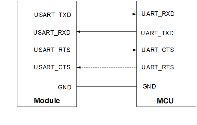
USART can be used as a UART application for AT command communication and data transmission. In this case, it supports a self-configurable baud rate with a default baud rate of 115200 bps. The USART connection between the module and the MCU is shown below. (The dotted lines are optional if required).
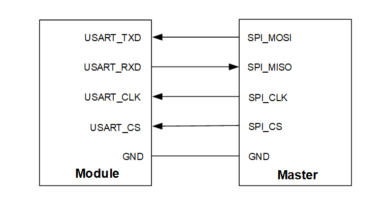
The following figure shows the USART connection between the module and the host when used as SPI application.
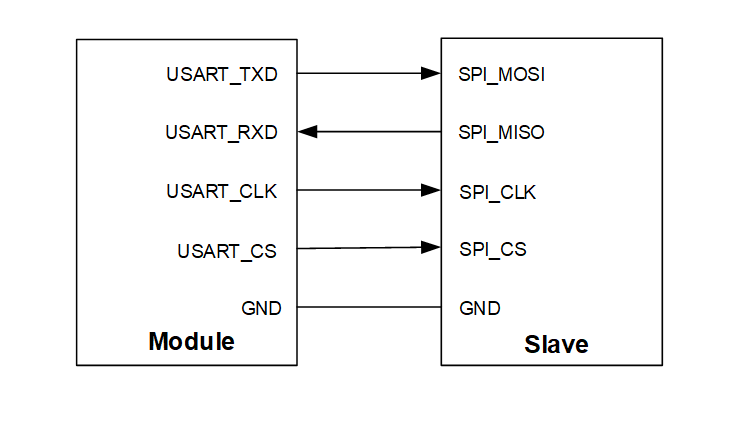
NOTE:
When USART is used as an SPI application, the input and output signals must be converted in slave mode: the receiver receives the signal hrough USART_TXD (SPI_MOSI), and the transmitter drives USART_RXD(SPI_MISO) to send the signal.
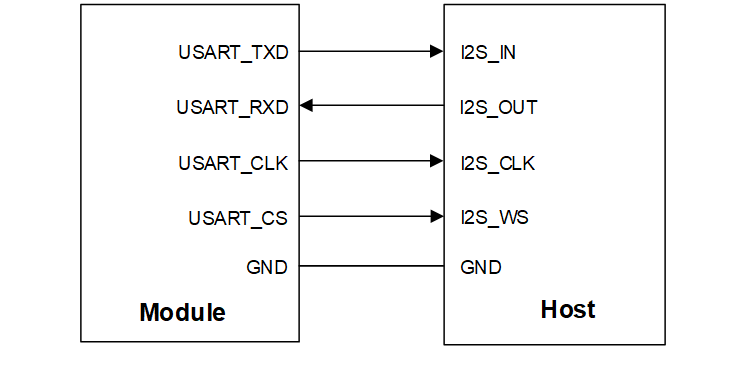
The following figure shows the USART connection between the module and the host when used as I2S application.
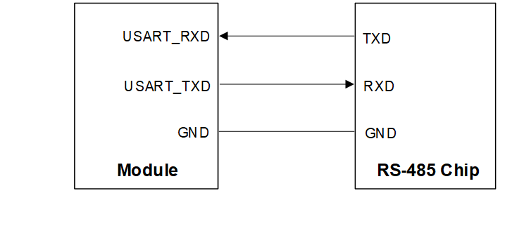
The following figure shows the USART connection between the module and the host when used as RS-485 application.
EUART
In the case of multiplexing, the module supports 1 EUART for high-speed UART and IrDA communication, and see Table 5 for more details.
- EUART has multiple modes of operation, with flexible configuration of frame format and baud rate. In multi-processor mode, EUART can remain idle when not addressed, helping to reduce power consumption and improve communication efficiency.
- EUART supports triple buffering and DMA (Direct Memory Access), and data transfer can be performed with minimal CPU usage, resulting in high-speed data transfer.
- EUART also supports the transmission and reception of large frame data in EM1 mode. In low- frequency EM2 mode, dedicated I/O ports can support data transmission and reception, allowing the module to maintain communication capabilities even in low-power states.
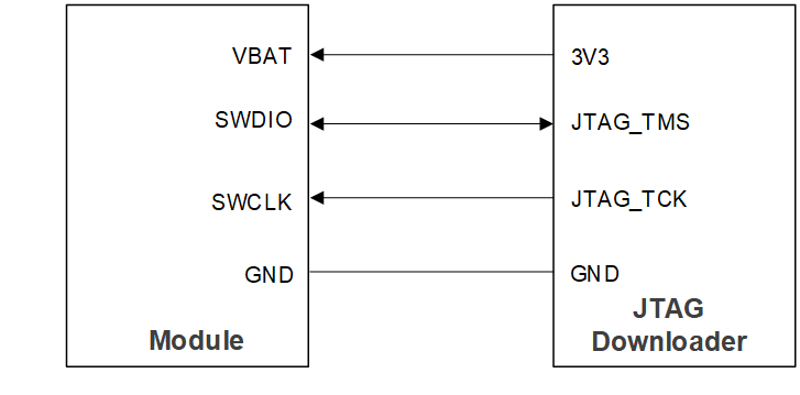
SWD Interface
The module supports a 2-pin SWD interface, the pin definitions are shown in the table below.
Pin Definition of SWD Interface:
| Pin Name | Pin No. | I/O | Description | Comment |
|---|---|---|---|---|
| SWDIO | 4 | DIO | Serial wire debugging input/output | Used for program downloading. Enabled after power-up. Internally pulled up to 3.3 V. |
| SWCLK | 3 | DI | Serial wire debugging clock | Used for program downloading. Enabled after power-up. Internally pulled down to GND. |
The SWD interface supports online program downloading and the common connection is shown below.
I2C Interfaces
In the case of multiplexing, the module can provide two I2C interfaces,both supporting master-slave mode and multi-master communication.Details of the interface multiplexing are shown in Table 5. The interface supports standard mode (100 kbps), fast mode (400 kbps) and fast mode + (1 Mbps), and also complies with slave device arbitration and timeout for compatibility with the SMBus system.Automatic identification of slave device addresses is supported in EM0~EM3 power modes.
Both the I2C interfaces are open-drain. The maximum value of the pull-up resistor (Rp) can be calculated by the maximal rise-time (Tr) for the given bus speed and the estimated bus capacitance (Cb) as shown below:
Rp = Tr / (0.8473 × Cb)
The maximal rise times for 100 kHz, 400 kHz and 1 MHz rate is 1 μs, 300ns and 120 ns respectively.
ADC Interface
In the case of multiplexing, the module supports one ADC interface, see Table 6 for more details. The interface supports up to 12-bit resolution at 1 million samples per second. The flexible incremental architecture uses oversampling, allowing applications to trade speed for higher resolution.
The key features of ADC interface are as below:
Flexible and configurable oversampling rate architecture, allowing trade-offs between rate and resolution:
- 1 Msps with oversampling ratio = 2
- 555 ksps with oversampling ratio = 4
- 76.9 ksps with oversampling ratio = 32Internal and external conversion trigger sources
- Immediate (software triggered)
- Local ADC timer
- External TIMER module (synchronous with output/PWM generation)
- General PRS hardware signalSelectable reference sources
- 1.21 V internal reference
- External precision reference
- Analog supply
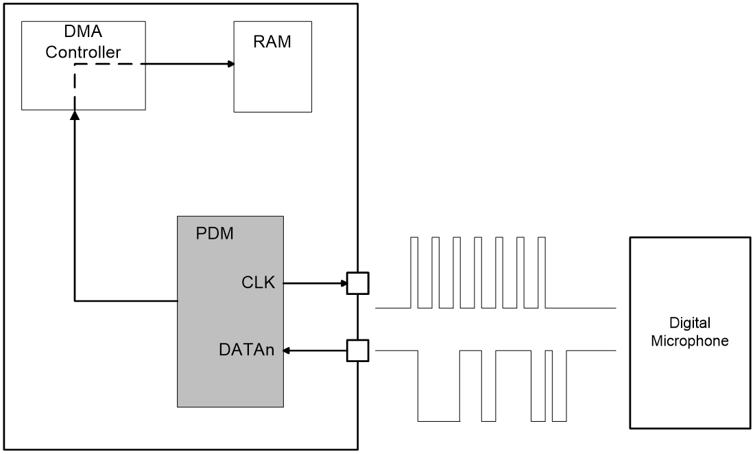
PDM Interface
In the case of multiplexing, the module supports one PDM interface, see Table 5 for more details. The PDM interface provides decimation filters for pulse-density modulated (PDM) microphones, isolated sigma-delta analogue-to-digital converters, digital sensors, and other PDM or sigma-delta bitstream peripherals. The decimation filter uses a programmable comb filter to decimate the incoming bitstream. PDM supports stereo or mono input and DMA transfers.
GPIO Interfaces
In the case of multiplexing, the module supports up to 18 GPIO interfaces, see Table 5 and Table 6 for more details. Each GPIO pin can be independently configured as input or output, as well as open-drain, open-source, glitch filtering, and other functions. Except for the SWD interface pins (SWDIO, SWCLK), the input and output functions of the other 16 GPIO pins are disabled after system reset.External resources such as timers, PWM, or USART_RDX/_TXD can be customised via the GPIO pins as required. The input value of a single pin can be configured to other peripherals via PRS or used to trigger external interrupts.
Operating Characteristics
Power Supply
Power supply pin and ground pins of the module are defined in the following table.
Pin Definition of Power Supply and GND Pins:
| Pin Name | Pin No. | I/O | Description | Min. | Typ. | Max. | Unit |
|---|---|---|---|---|---|---|---|
| VBAT | 2 | PI | Power supply for the module | 1.71 | 3.3 | 3.8 | V |
| GND | 1, 8, 9 |
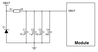
Reference Design for Power Supply
The module is powered by VBAT, and it is recommended to use a power supply chip that can provide sufficient current of at least 20 mA. For better power supply performance, it is recommended to parallel a 22 μF decoupling capacitor, and two filter capacitors (1 μF and 100 nF) near the module's VBAT pin. C4 is reserved for debugging and not mounted by default. In addition, it is recommended to add a TVS near the VBAT to improve the surge voltage bearing capacity of the module. In principle,the longer the VBAT trace is, the wider it should be.
VBAT reference circuit is shown below:
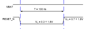
Reset
Pull the RESET_N low for at least 100 ns and then release it to reset the module.
Pin Definition of RESET_N:
| Pin Name | Pin No. | I/O | Description | Comment |
|---|---|---|---|---|
| RESET_N | 5 | DI | Reset the module | Hardware reset. Internally pulled up to 1.8 V. Active low. |
The reference design for resetting the module is shown below. Press the button directly to realize the resetting of the module. At the same time, it is recommended to place a TVS near the button for ESD protection and a 100 nF capacitor to avoid jittering.
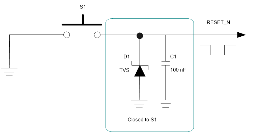
The module reset timing is illustrated in the following figure.
RF Performances
Bluetooth Performances
Bluetooth Performances:
| Operating Frequency | ||
|---|---|---|
| 2.400--2.4835 GHz | ||
| Modulation | ||
| GFSK | ||
| Operating Mode | ||
| BLE | ||
| Condition (VBAT = 3.3 V;Temp. 25 °C) | Transmitting Power | Receiver Sensitivity |
| BLE (1 Mbps) | ≤ 6 dBm | -98 dBm ±2 dB |
| BLE (2 Mbps) | ≤ 6 dBm | -95 dBm ±2 dB |
| BLE (S = 2) 8 | ≤ 6 dBm | -102 dBm ±2 dB |
| BLE (S = 8) | ≤ 6 dBm | -106 dBm ±2 dB |
PCB Antenna
The module supports PCB antenna and the antenna specifications are shown below:
PCB Antenna Specifications:
| Parameter | Specification |
|---|---|
| Frequency Range (GHz) | 2.400--2.500 |
| Input Impedance (Ω) | 50 (Typ.) |
| VSWR | ≤ 2 |
| Gain (dBi) | -0.5 (Max.) |
| Efficiency | 30 % (Avg.) |
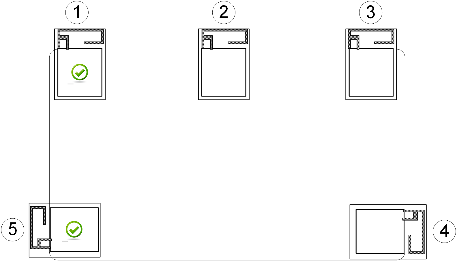
The performance of the PCB antenna depends on the entire product,including the motherboard, case, and other RF signals, and it is recommended to verify it at the early stage of design. To ensure the performance and reliability when designed with PCB antenna, follow the basic principles below for module's placement and layout:
- The module should be placed on the edge of the motherboard.
- On the motherboard, all PCB layers under the PCB antenna should be designed as keepout areas.
- On the motherboard, ensure a minimum clearance of 16 millimeters between the PCB antenna and vias, traces, copper pour area, and other components, such as connectors, Ethernet ports and any metal components.
- If using a plastic case, ensure a minimum clearance of 10millimeters between the PCB antenna and the plastic case. If using a metal case, it is recommended to use an external antenna.
NOTE:
If any of the above principles cannot be guaranteed, it is advisable to explore alternative antenna solutions for the module or seek assistance from the Quectel Antenna Team, who can offer design assistance and recommend suitable external antennas. Please feel free to contact Quectel Technical Support if necessary.
It is recommended to place the module at areas 1 and 5 as showing in the figure bellow.
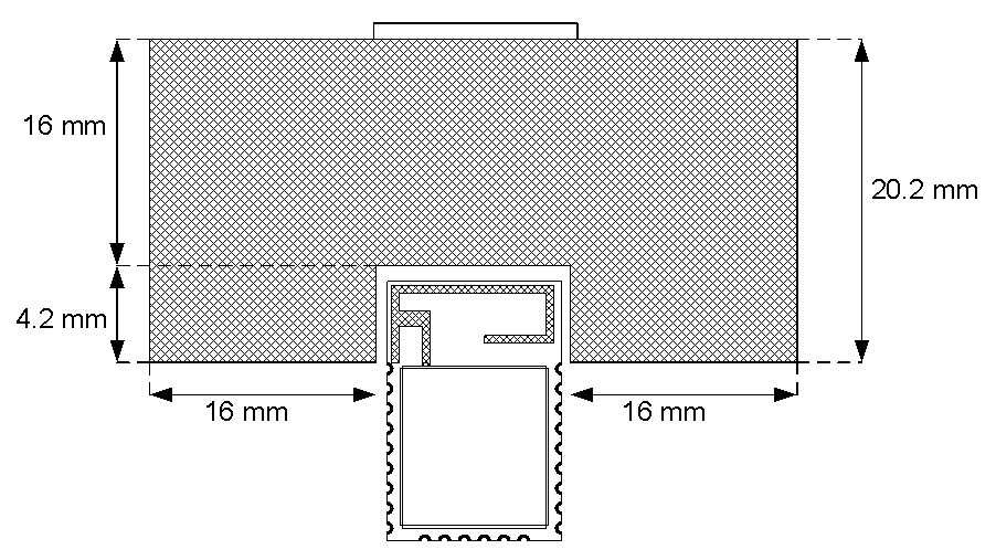
To ensure module performance, do not route at the RF test point at thebottom of the module during PCB design. The prohibited area during routing is shown in the red box below:
Electrical Characteristics & Reliability
Absolute Maximum Ratings
Absolute maximum ratings for power supply and voltage on digital and analog pins of the module are listed in the following table.
Absolute Maximum Ratings (Unit: V):
| Parameter | Min. | Max. |
|---|---|---|
| VBAT | -0.3 | 3.8 |
| Voltage at Digital Pins | -0.3 | 4.1 |
Power Supply Ratings
Module Power Supply Ratings (Unit: V):
| Parameter | Description | Condition | Min. | Typ. | Max. |
|---|---|---|---|---|---|
| VBAT | Power supply for the module | The actual input voltages must be kept between the minimum and maximum values. | 1.71 | 3.3 | 3.8 |
Bluetooth Power Consumption
Bluetooth Consumption (Unit: mA):
| Mode | Typ. | Max. | Unit |
|---|---|---|---|
| Sleep Mode | - | 1.769 | μA |
| BLE 1 Mbps @ Tx 6 dBm | 6.722 | 7.532 | mA |
| BLE 2 Mbps @ Tx 6 dBm | 4.630 | 5.471 | mA |
| BLE S = 2 @ Tx 6 dBm9 | 6.074 | 8.648 | mA |
| BLE S = 8 @ Tx 6 dBm | 7.847 | 9.030 | mA |
Digital I/O Characteristics
VBAT I/O Characteristics (Unit: V):
| Parameter | Description | Min. | Max. |
|---|---|---|---|
| VIH | High-level input voltage | 0.7 × VBAT | - |
| VIL | Low-level input voltage | - | 0.3 × VBAT |
| VOH | High-level output voltage | 0.8 × VBAT | - |
| VOL | Low-level output voltage | - | 0.2 × VBAT |
NOTE:
VBAT = 3.3 V.
ESD Protection
Static electricity occurs naturally and may damage the module.Therefore, applying proper ESD countermeasures and handling methods is imperative. For example, wear anti-static gloves during the development,production, assembly and testing of the module; add ESD protection components to the ESD sensitive interfaces and points in the product design.
Mechanical Information
This chapter describes the mechanical dimensions of the module. All dimensions are measured in millimeters (mm), and the dimensional tolerances are ±0.2 mm unless otherwise specified.
Mechanical Dimensions
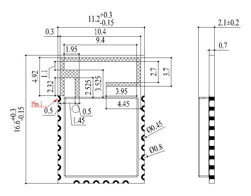
NOTE:
The module's coplanarity standard: ≤ 0.13 mm.
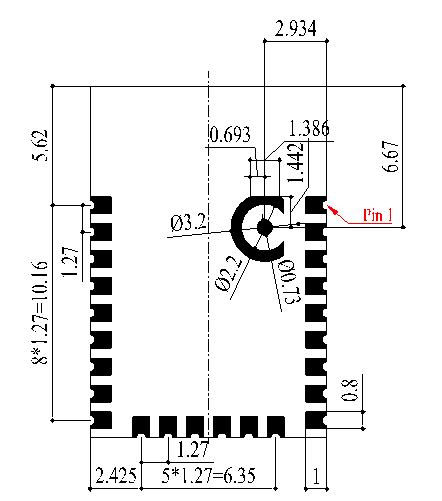
Recommended Footprint
NOTE:
Keep at least 3 mm between the module and other components on the motherboard to improve soldering quality and maintenance convenience.
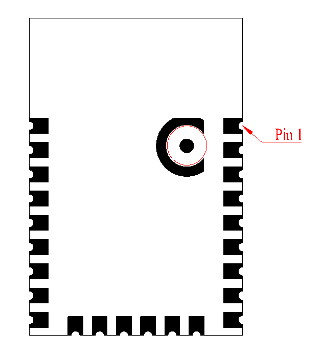
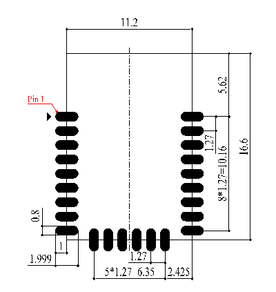
Top and Bottom Views
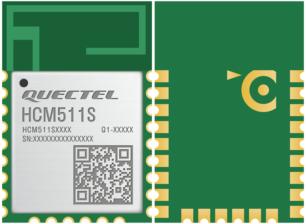
NOTE:
Images above are for illustrative purposes only and may differ from the actual module. For authentic appearance and label, please refer to the module received from Quectel.
Storage and Packaging
Storage Conditions
The module is provided with vacuum-sealed packaging. MSL of the module is rated as 3. The storage requirements are shown below.
- Recommended Storage Condition: the temperature should be 23 ±5 °C and the relative humidity should be 35--60 %.
- Shelf life (in a vacuum-sealed packaging): 12 months in Recommended Storage Condition.
- Floor life: 168 hours 10 in a factory where the temperature is 23±5 °C and relative humidity is below 60 %. After the vacuum-sealed packaging is removed, the module must be processed in reflow soldering or other high-temperature operations within 168 hours.Otherwise, the module should be stored in an environment where the relative humidity is less than 10 % (e.g., a dry cabinet).
- The module should be pre-baked to avoid blistering, cracks and inner-layer separation in PCB under the following circumstances:
- The module is not stored in Recommended Storage Condition;
- Violation of the third requirement mentioned above;
- Vacuum-sealed packaging is broken, or the packaging has been removed for over 24 hours;
- Before module repairing.
- If needed, the pre-baking should follow the requirements below:
- The module should be baked for 8 hours at 120 ±5 °C;
- The module must be soldered to PCB within 24 hours after the baking,otherwise it should be put in a dry environment such as in a drycabinet.
NOTE:
- To avoid blistering, layer separation and other soldering issues, extended exposure of the module to the air is forbidden.
- Take out the module from the package and put it on high-temperature-resistant fixtures before baking. If shorter baking time is desired, see IPC/JEDEC J-STD-033 for the baking procedure.
- Pay attention to ESD protection, such as wearing anti-static gloves, when touching the modules.
Manufacturing and Soldering
Push the squeegee to apply the solder paste on the surface of stencil,thus making the paste fill the stencil openings and then penetrate to the PCB. Apply proper force on the squeegee to produce a clean stencil surface on a single pass. To guarantee module soldering quality, the thickness of stencil for the module is recommended to be 0.15--0.18 mm.For more details, see document [3].
The recommended peak reflow temperature should be 235--246 ºC, with 246ºC as the absolute maximum reflow temperature. To avoid damage to the module caused by repeated heating, it is recommended that the module should be mounted only after reflow soldering for the other side of PCB has been completed. The recommended reflow soldering thermal profile(lead-free reflow soldering) and related parameters are shown below.
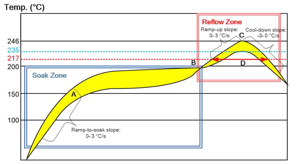
Recommended Thermal Profile Parameters:
| Factor | Recommended Value |
|---|---|
| Soak Zone | |
| Ramp-to-soak slope | 0--3 °C/s |
| Soak time (between A and B: 150 °C and 200 °C) | 70--120 s |
| Reflow Zone | |
| Ramp-up slope | 0--3 °C/s |
| Reflow time (D: over 217 °C) | 40--70 s |
| Max. temperature | 235--246 °C |
| Cool-down slope | -3--0 °C/s |
| Reflow Cycle | |
| Max. reflow cycle | 1 |
NOTE:
- The above profile parameter requirements are for the measured temperature of solder joints. Both the hottest and coldestspots of solder joints on the PCB should meet the aboverequirements.
- During manufacturing and soldering, or any other processes that may contact the module directly, NEVER wipe the module'sshielding can with organic solvents, such as acetone, ethyl alcohol, isopropyl alcohol, trichloroethylene, etc. Otherwise, the shielding can may become rusted.
- The shielding can for the module is made of Cupro-Nickel base material. It is tested that after 12 hours' Neutral Salt Spray test, the laser engraved label information on the shielding can is still clearly identifiable and the QR code is still readable, although white rust may be found.
- If a conformal coating is necessary for the module, do NOT use any coating material that may chemically react with the PCB or shielding cover, and prevent the coating material from flowing into the module.
- Avoid using ultrasonic technology for module cleaning since it can damage crystals inside the module.
- Avoid using materials that contain mercury (Hg), such as adhesives, for module processing, even if the materials are RoHS compliant and their mercury content is below 1000 ppm (0.1%).
- Corrosive gases may corrode the electronic components inside the module, affecting their reliability and performance, and potentially leading to a shortened service life that fails to meet the designed lifespan. Therefore, do not store or use unprotected modules in environments containing corrosive gases such as hydrogen sulfide, sulfur dioxide, chlorine, and ammonia.
- Due to the complexity of the SMT process, please contact Quectel Technical Support in advance for any situation that you are not sure about, or any process (e.g. selective soldering,ultrasonic soldering) that is not mentioned in document [4].
Packaging Specification
This chapter outlines the key packaging parameters and processes. All figures below are for reference purposes only, as the actual appearance and structure of packaging materials may vary in delivery.
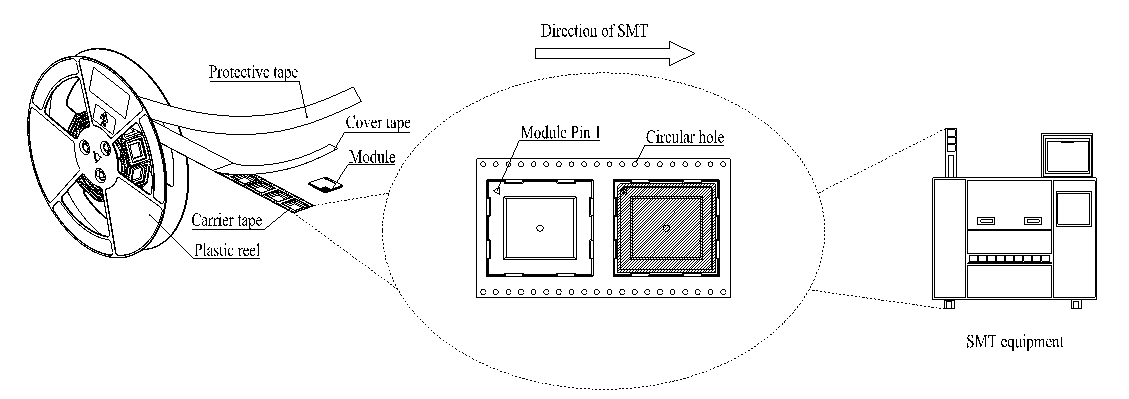
The modules are packed in a tape and reel packaging as specified in the sub-chapters below.
Carrier Tape
Carrier tape dimensions are illustrated in the following figure and table:
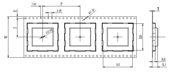
Carrier Tape Dimension Table (Unit: mm):
| W | P | T | A0 | B0 | K0 | K1 | F | E |
|---|---|---|---|---|---|---|---|---|
| 32 | 24 | 0.4 | 11.6 | 17 | 2.6 | 4.6 | 14.2 | 1.75 |
Plastic Reel
Plastic reel dimensions are illustrated in the following figure and table:
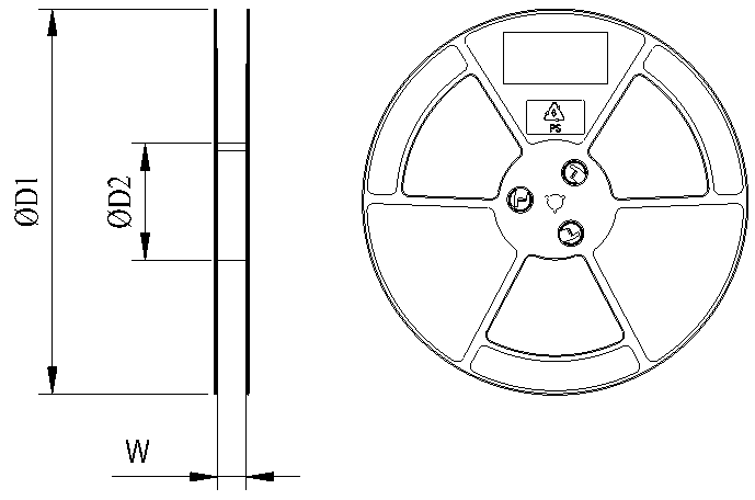
Plastic Reel Dimension Table (Unit: mm):
| øD1 | øD2 | W |
|---|---|---|
| 330 | 100 | 32.5 |
Mounting Direction
Packaging Process
Packaging Process:
| Image | Description |
|---|---|
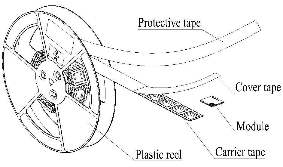 |
Place the modules onto the carrier tape cavity and cover them securely with cover tape. Wind the heat-sealed carrier tape onto a plastic reel and apply a protective tape for additional protection. 1 plastic reel can pack 500 modules. |
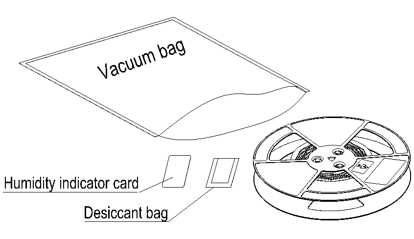 |
Place the packaged plastic reel, humidity indicator card and desiccant bag into a vacuum bag, and vacuumize it. |
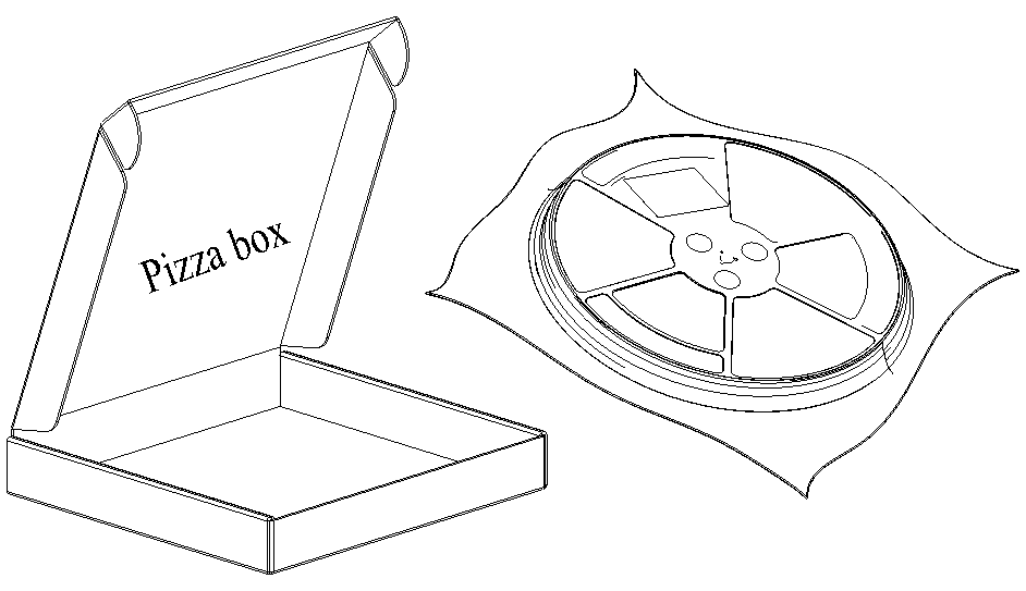 |
Place the vacuum-packed plastic reel into a pizza box. |
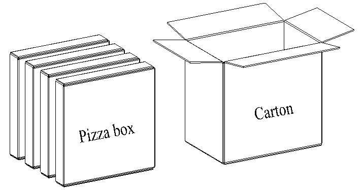 |
Place the 4 packaged pizza boxes into 1 carton and seal it. 1 carton can pack 2000 modules. |
Appendix References
Reference Documents:
| Document Name |
|---|
| [1]Quectel_HCM511S_TE-B_User_Guide |
| [2]Quectel_HCM511S_AT_Commands_Manual |
| [3]Quectel_Module_Stencil_Design_Requirements |
| [4]Quectel_Module_SMT_Application_Note |
Terms and Abbreviations:
| Abbreviation | Description |
|---|---|
| ADC | Incremental Analog to Digital Converter |
| ARM | Advanced RISC Machine |
| BLE | Bluetooth Low Energy |
| CDM | Charged Device Model |
| CMU | Clock Management Unit |
| CPU | Central Processing Unit |
| DC | Direct Current |
| DMA | Direct Memory Access |
| EM | Energy Mode |
| ESD | Electrostatic Discharge |
| ETM | Embedded Trace Macrocell |
| EUART | Enhanced Universal Asynchronous Receiver/Transmitter |
| FRC | Frame Controller |
| GFSK | Gauss frequency Shift Keying |
| GND | Ground |
| GPIO | General-Purpose Input/Output |
| HBM | Human Body Mode |
| I2C | Inter-Integrated Circuit |
| I2S | Inter-IC Sound |
| I/O | Input/Output |
| IrDA | Infra-red Data Association |
| JTAG | Joint Test Action Group |
| LCC | Leadless Chip Carrier (package) |
| Mbps | Million Bits Per Second |
| MCU | Microcontroller Unit |
| MISO | Master In Slave Out |
| MOSI | Master Out Slave In |
| OTA | Over-The-Air |
| PCB | Printed Circuit Board |
| PDM | Pulse Density Modulation |
| PRS | Peripheral Reflex System |
| PWM | Pulse Width Modulation |
| RAM | Random Access Memory |
| RF | Radio Frequency |
| RoHS | Restriction of Hazardous Substances |
| SPI | Serial Peripheral Interface |
| SWD | Serial Wire Debug |
| TVS | Transient Voltage Suppressor |
| Tx | Transmit |
| UART | Universal Asynchronous Receiver/Transmitter |
| USART | Universal Synchronous/Asynchronous Receiver/Transmitter |
| (U)SIM | (Universal) Subscriber Identity Module |
| VIH | High-level Input Voltage |
| VIL | Low-level Input Voltage |
| Vmax | Maximum Voltage |
| Vmin | Minimum Voltage |
| Vnom | Nominal Voltage |
| VOH | High-level Output Voltage |
| VOL | Low-level Output Voltage |
| VSWR | Voltage Standing Wave Ratio |
The module supports 352 KB or 512 KB flash. For more details,please contact Quectel Technical Support.↩
Only supported by module model with built-in 512 KB Flash.↩
Within the operating temperature range, the module's related performance meets Bluetooth specifications.↩
Quectel supplies an evaluation board (HCM511S-TE-B) with accessories to develop and test the module. For more details, see document [1].↩
For more details about the interfaces, see Chapter 3.3 and Chapter 3.4.↩
In the standard firmware version, it is the "sleep wake-up control" function. The default high level, pull this pin low for more than 40 ms to put the module into sleep mode; in sleep mode,pull this pin high for more than 40 ms to wake up the module.↩
In the standard firmware version, this is the "message notification indicator" function. For detailed configuration,please refer to document [2].↩
Only supported by module model with built-in 512 KB Flash.↩
Only supported by module model with built-in 512 KB Flash.↩
This floor life is only applicable when the environment conforms to IPC/JEDEC J-STD-033. It is recommended to start the solderreflow process within 24 hours after the package is removed if the temperature and moisture do not conform to, or are not sure to conform to IPC/JEDEC J-STD-033. Do not unpack the modules in large quantities until they are ready for soldering.↩