

 English
HCM511S TE-B User Guide
Introduction
For convenient development of applications with Quectel HCM511S, Quectel supplies the corresponding development board (HCM511S-TE-B) for module testing. This document can help you quickly understand HCM511S-TE-B interface specifications, RF characteristics, electrical and mechanical details and how to effectively use it.
Product Overview
HCM511S-TE-B is a Bluetooth development board that supports a series of interfaces. It can be used for testing basic functionalities and developing HCM511S.
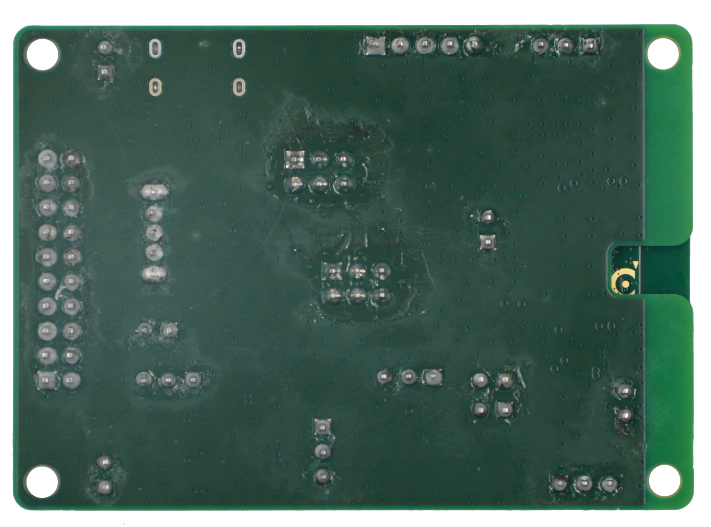
Top and Bottom Views
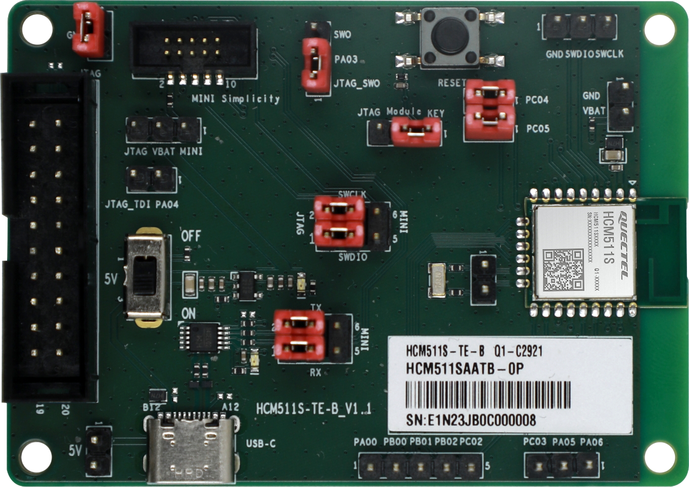
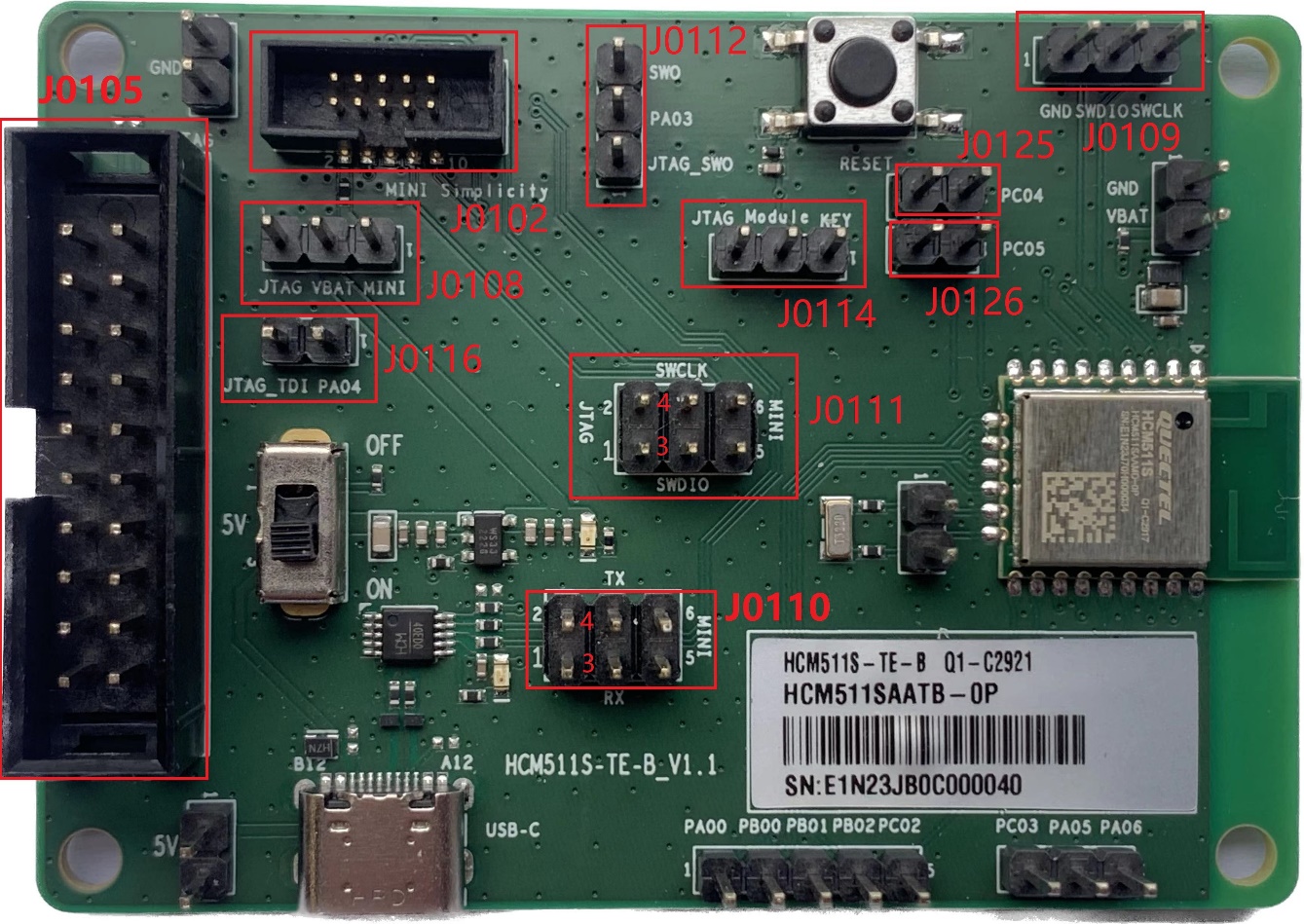
Component Placement
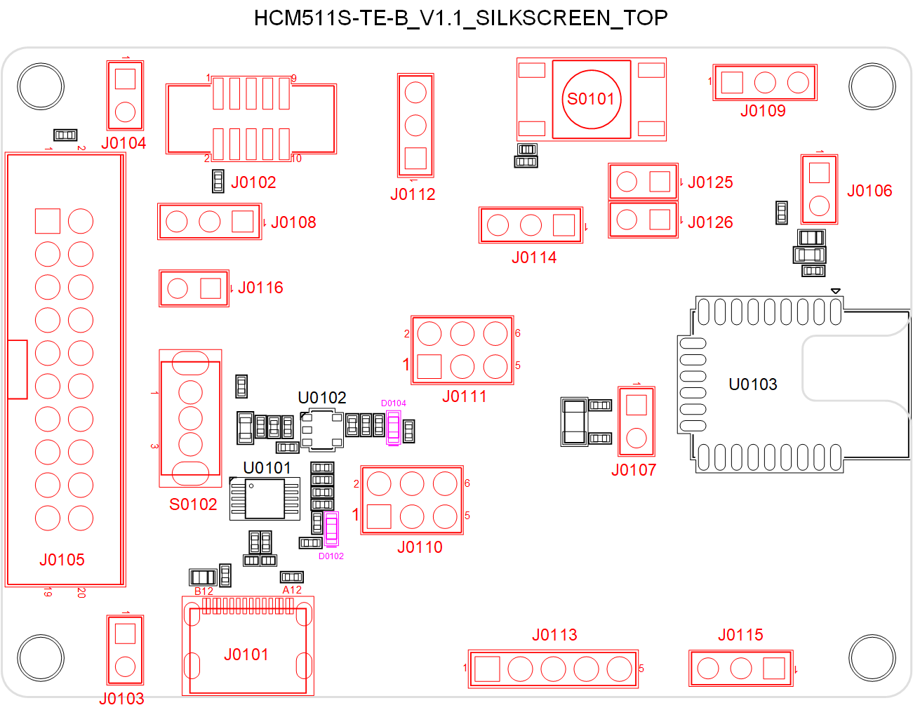
Component Information:
| Component | RefDes. | Description |
|---|---|---|
| Module | U0103 | HCM511S module |
| LDO | U0102 | 5 V to 3.3 V |
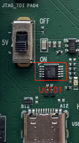
| USB-to-UART Bridge | U0101 | USB-to-UART bridge |
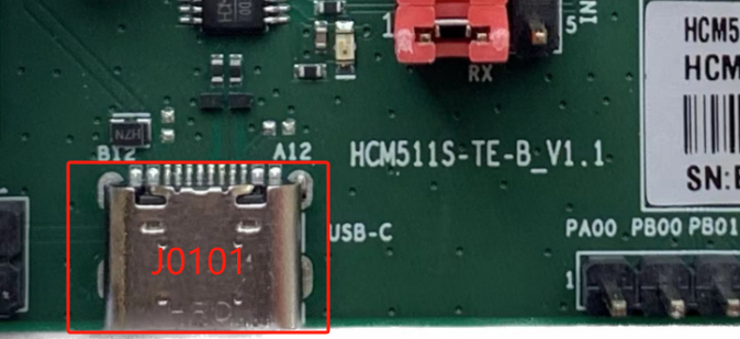
| Power Supply Interfaces | J0101 | USB Type-C power supply interface |
| Power Supply Interfaces | J0103 | Positive electrode of external power supply interface (+5 V) |
| Power Supply Interfaces | J0104 | Negative electrode of external power supply interface (GND) |
| Power Supply Interfaces | J0108 | VBAT jumper interface |
| Power Switch | S0102 | VBAT ON/OFF control |
| Reset Button | S0101 | Resets the module via J0114 |
| USB Interface | J0101 | Connects to USART interface of the module via U0101 and J0110 |
| Status LEDs | D0104 | Indicates VBAT ON/OFF status |
| Status LEDs | D0102 | Indicates USART status |
| Debug Interfaces | J0109 | 3-pin SWD interface |
| Debug Interfaces | J0105 | 20-pin JTAG interface |
| Debug Interfaces | J0102 | 10-pin mini simplicity interface |
| Test Points | J0106 | Tests the module power consumption by connecting an external programmable power supply |
| Test Points | J0107,J0113, J0115 | Test basic functions |
| PA03 Jumper Interface | J0112 | Connections between different jumper pins for J0105/J0102 |
| SWD Jumper Interface | J0111 | Connections between different jumper pins for J0105/J0102 |
| USART Jumper Interface | J0110 | Connections between different jumper pins for U0101/J0102 |
| Reset Jumper Interface | J0114 | Connections between different jumper pins for S0101/J0105/J0102 |
| PA04 Jumper Interface | J0116 | Connections between jumper pins for J0105 |
| PC04 Jumper Interface | J0125 | Connections between jumper pins for J0102 |
| PC05 Jumper Interface | J0126 | Connections between jumper pins for J0102 |
NOTE:
See Chapter 4 for details of pins connection of each jumper interface in the table above.
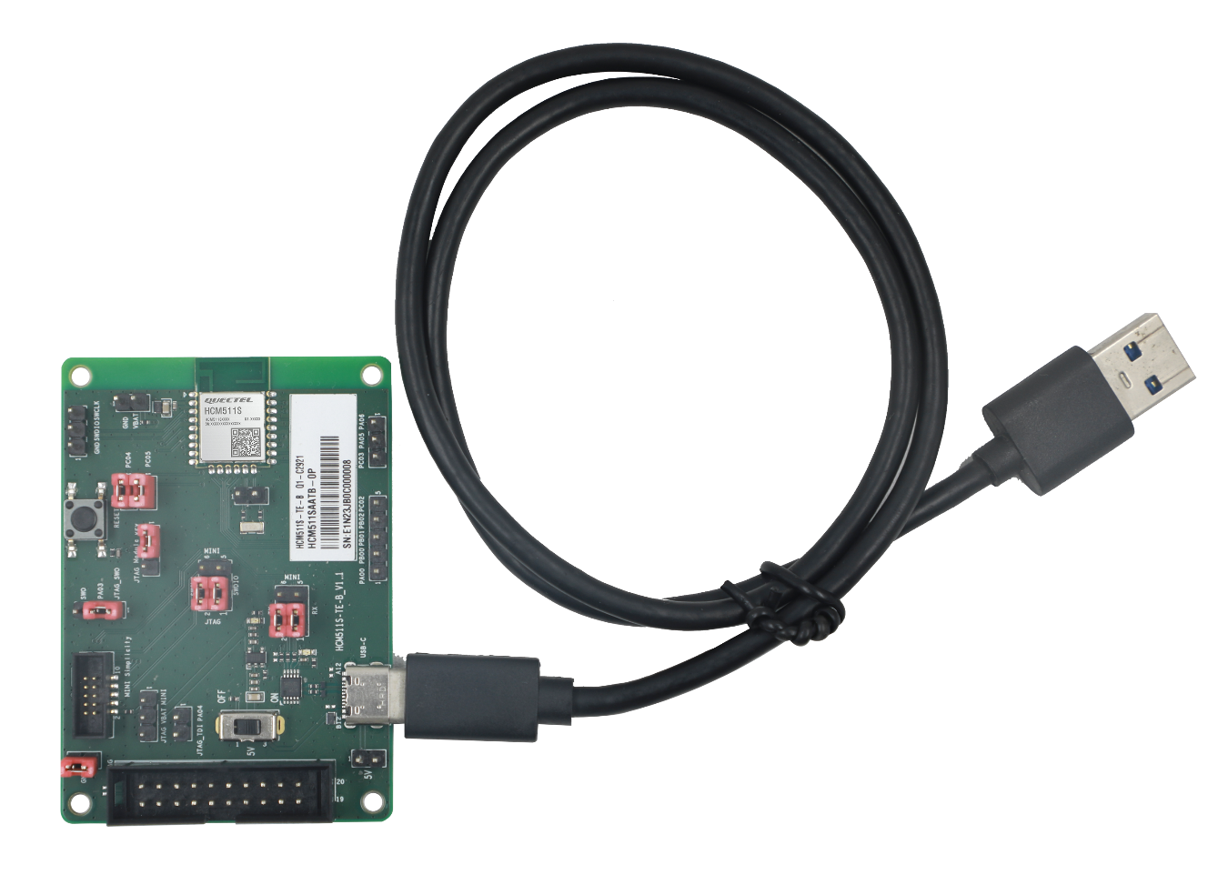
Kit Accessory & Assembly
Kit Accessory
Accessory List:
| Items | Description | Quantity (pcs) |
|---|---|---|
| Cable | USB Type-C cable | 1 |
Kit Assembly
Interface Applications
This chapter outlines the information and applications of some hardware interfaces of HCM511S-TE-B.
Power Supply Interfaces
The simplified schematic of HCM511S-TE-B is shown in the following figure.
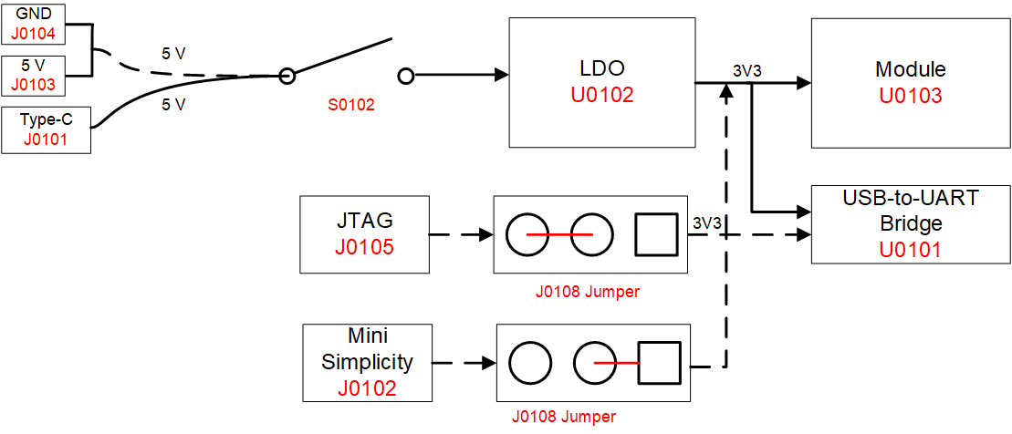
Power Switch and Reset Button
HCM511S-TE-B includes one power switch (S0102) and one reset button(S0101) as shown in the following figure.
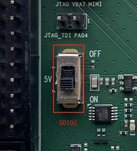
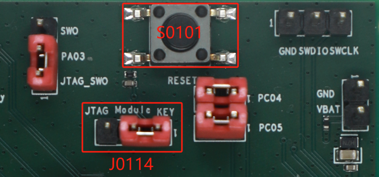
Description of Power Switch and Reset Button:
| RefDes. | Description |
|---|---|
| S0101 | Resets the module via J0114 |
| S0102 | VBAT ON/OFF control |
| J0114 | Connects Module to KEY |
USB Interface
HCM511S-TE-B integrates J0101 (USB interface) connecting to the module's USART interface via U0101 (USB-to-UART bridge) for USB-to-UART connection, with the jumpers on J0110 as shown in the following figure.
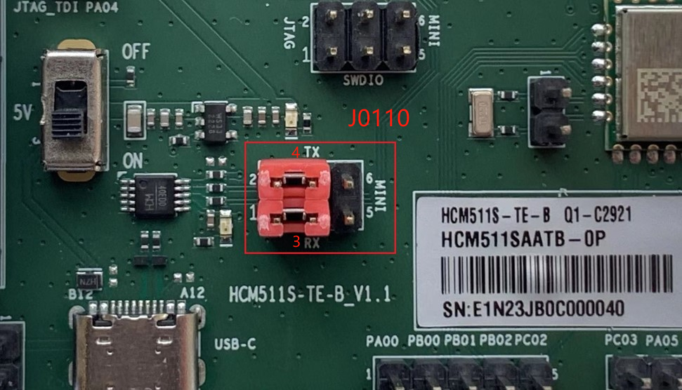
J0101 supports 115200 bps baud rate by default. It is intended for data transmission between the module and the host. It can also be used for AT command communication and debugging.
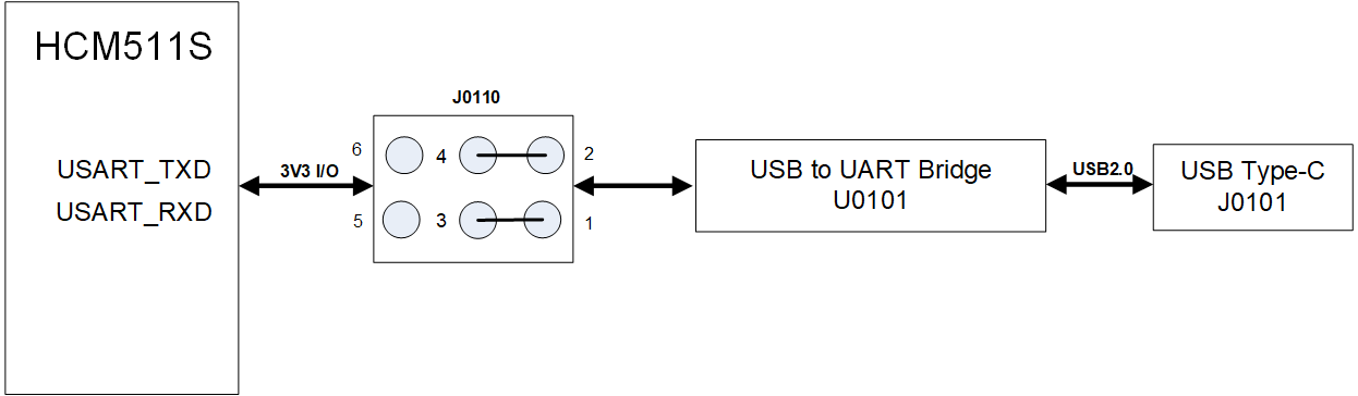
Description of USB-to-UART Connection:
| RefDes. | Description |
|---|---|
| U0101 | USB-to-UART bridge |
| J0101 | USB interface |
| J0110 | Connects pin 1 to pin 3 |
| J0110 | Connects pin 2 to pin 4 |
Debug Interfaces
The module supports J0109 (SWD interface), J0105 (JTAG interface) and J0102 (mini simplicity connector) for flash programming and normal debugging.
Description of Debug and Jumper Interfaces:
| RefDes. | Description |
|---|---|
| J0109 | 3-pin SWD interface |
| J0105 | 20-pin JTAG interface |
| J0102 | 10-pin mini simplicity interface |
| J0108 | Connects VBAT to JTAG for JTAG connection |
| J0108 | Connects VBAT to MINI for mini simplicity connection |
| J0116 | Connects JTAG_TDI to PA04 for JTAG connection |
| J0112 | Connects PA03 to JTAG_SWO for JTAG connection |
| J0112 | Connects PA03 to SWO for mini simplicity connection |
| J0114 | Connects Module to JTAG for JTAG connection |
| J0114 | Connects Module to KEY for mini simplicity connection |
| J0111 | Connects pin1 to pin 3 and pin 2 to pin 4 for JTAG connection |
| J0111 | Connects pin 4 to pin 6 and pin 3 to pin 5 for mini simplicity connection |
| J0110 | Connects pin 4 to pin 6 and pin 3 to pin 5 for mini simplicity connection |
| J0125 | Connects pin 1 to pin 2 for mini simplicity connection |
| J0126 | Connects pin 1 to pin 2 for mini simplicity connection |
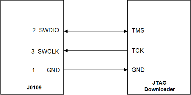
When you use J0109 (SWD interface), connect pin 1 (GND), pin 2 (SWDIO) and pin 3 (SWCLK) of J0109 to JTAG downloader as below:
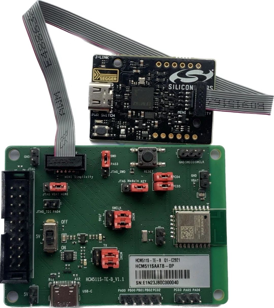
When you use J0105 (JTAG interface), place the jumper as shown below,and connect the JTAG downloader to PC through a USB type-C cable.
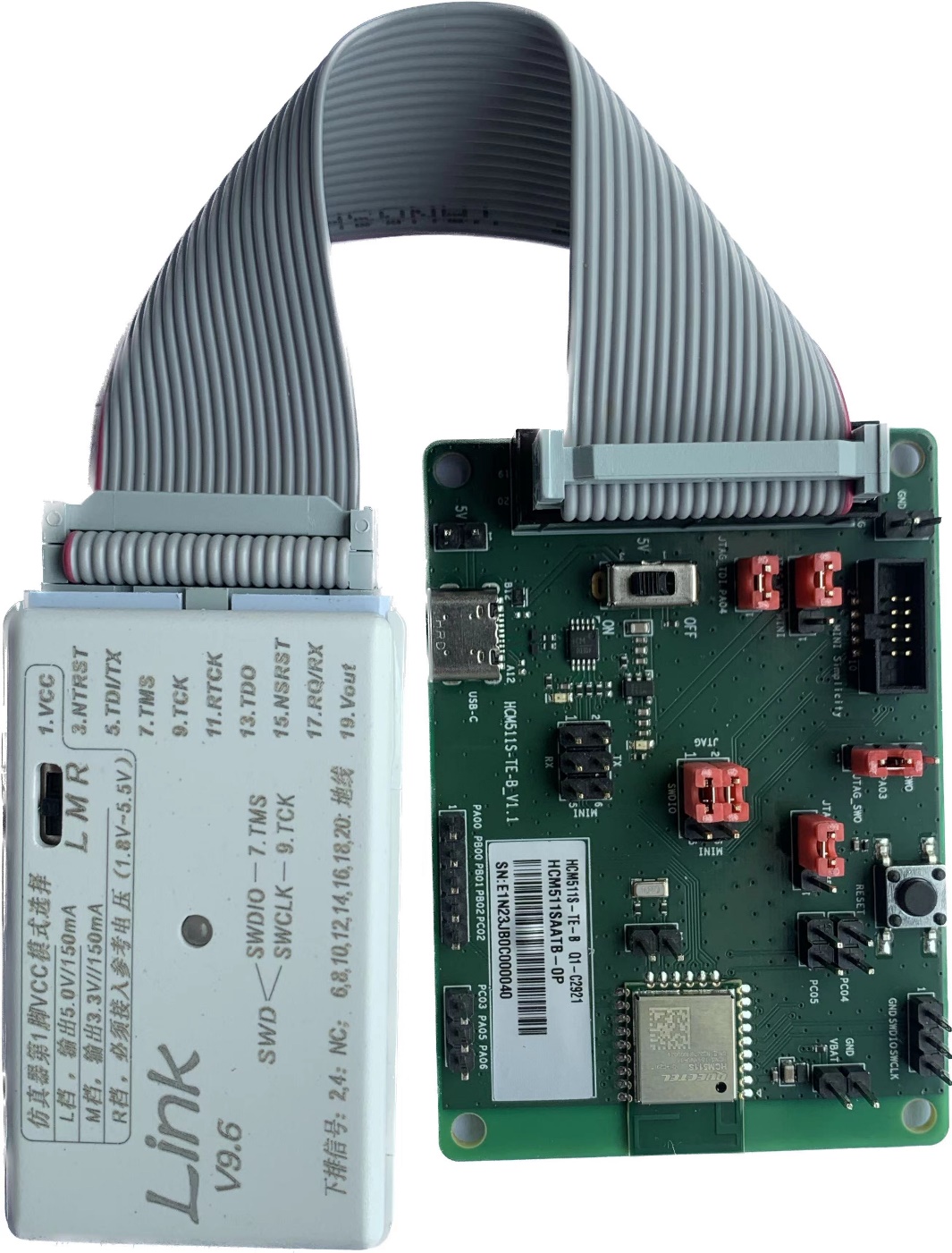
When you use J0102 (mini simplicity interface), place the jumper as shown below, and connect the J-link debugger (SI-DBG1015A) to PC through a USB type-C cable.
RF Interfaces
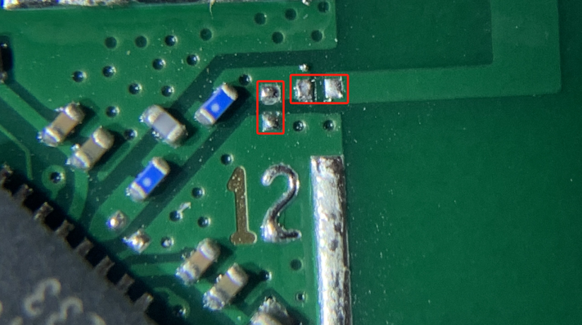
Test the conductivity through the concentric circle on the bottom side.Weld the RF coaxial cable as shown below.
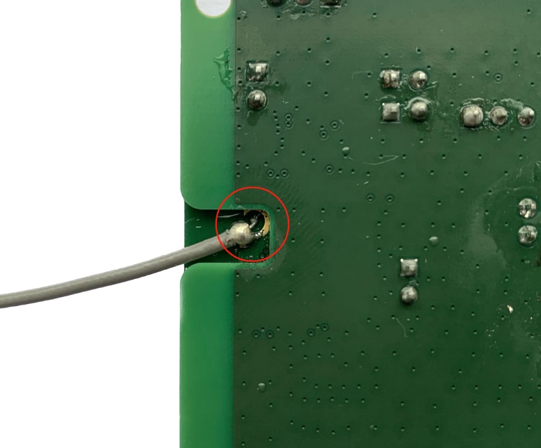
Before testing the conductivity, you must remove the shielding cover of the module and matched resistor and capacitor to disconnect the matching circuit of the PCB antenna. The matched resistor and capacitor are shown as below.
Test Points
HCM511S-TE-B features a series of test points (J0106, J0107, J0113, J0115), which are illustrated in the following figure, and these test points can help you to obtain the corresponding waveform of some signals.
To test the module's power consumption, disconnect the resistor indicated by the red arrow and connect pin 1 of J0106 to the negative pole and pin 2 of J0106 to the positive pole for the programmable power supply.
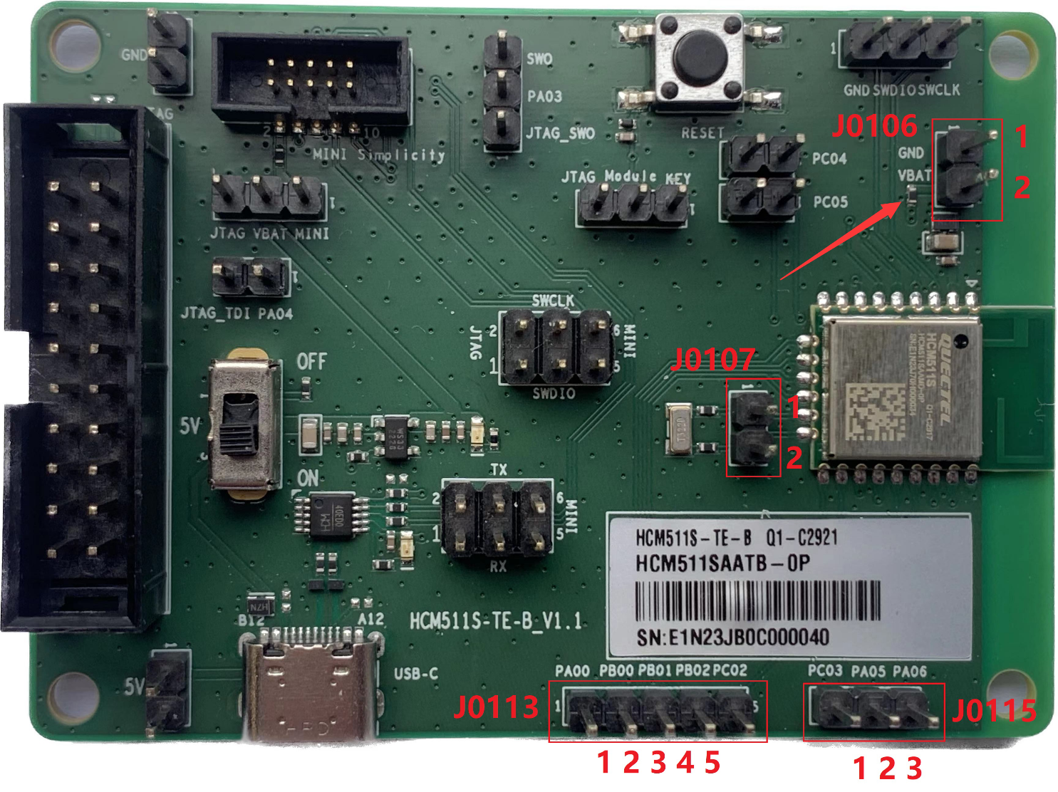
Pin Description of Test Points:
J0106:
| Pin No. | Pin Name | Description |
|---|---|---|
| 1 | GND | Connects these two pins to an external programmable power supply to test the module power consumption |
| 2 | VBAT | Connects these two pins to an external programmable power supply to test the module power consumption |
J0107:
| Pin No. | Pin Name | Description |
|---|---|---|
| 1 | - | Connected directly to module's GPIO14 |
| 2 | - | Connected directly to module's GPIO13 |
J0113:
| Pin No. | Pin Name | Description |
|---|---|---|
| 1 | PA00 | Connected directly to module's GPIO1 |
| 2 | PB00 | Connected directly to module's GPIO6 |
| 3 | PB01 | Connected directly to module's GPIO7 |
| 4 | PB02 | Connected directly to module's GPIO8 |
| 5 | PC02 | Connected directly to module's GPIO9 |
J0115:
| Pin No. | Pin Name | Description |
|---|---|---|
| 1 | PC03 | Connected directly to module's GPIO10 |
| 2 | PA05 | Connected directly to module's GPIO4 |
| 3 | PA06 | Connected directly to module's GPIO5 |
NOTE:
See document [1] for details of module pin names and definitions in the above table.
Status LEDs
HCM511S-TE-B comprises 2 status LEDs, which are presented in the following figure.
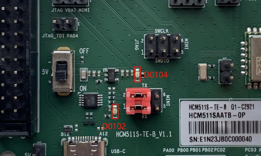
Description of Status LEDs:
| RefDes. | Description | Comment |
|---|---|---|
| D0102 | Indicates USART status | Light on: power on Flicker: data transmission |
| D0104 | VBAT ON/OFF indicator | Light on: power on Light off: power off |
Operating Procedures
This chapter outlines how to use the HCM511S-TE-B for testing and evaluating the module.
Power Up
- Connect J0101 (USB interface) of HCM511S-TE-B to the PC with the USB Type-C cable.
- Switch S0102 (Power Switch) to ON state, then D0104 (VBAT ON/OFF indicator) will light up.
Communication via USB Connector
- Turn on the module according to the procedures referred to in Chapter 5.1.
- The USB serial port number can be viewed through the PC Device Manager, as shown below.
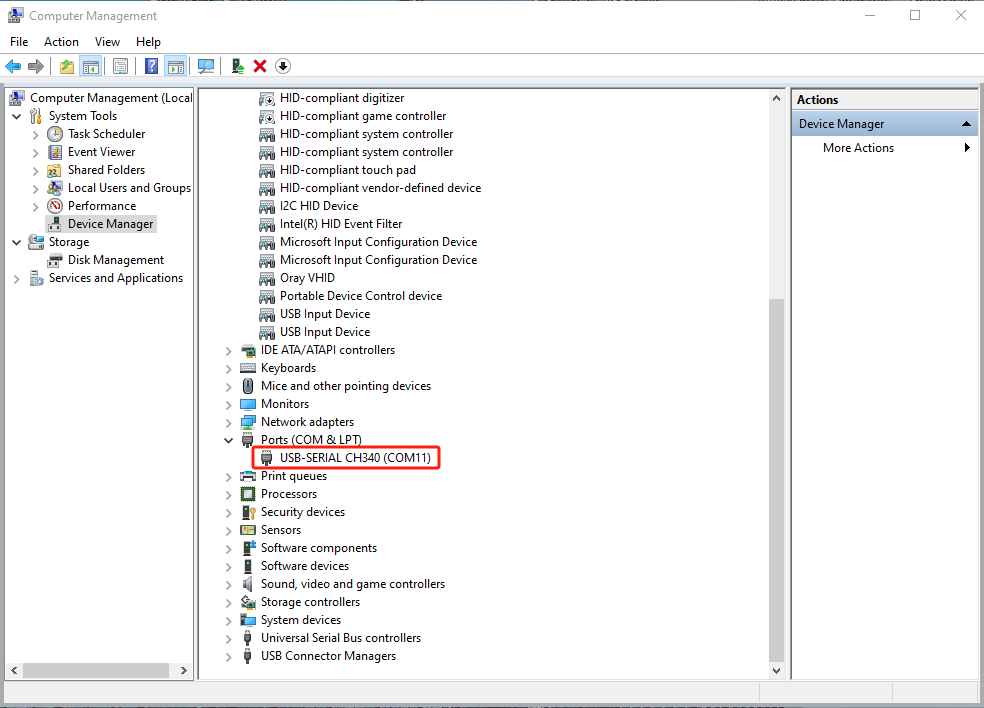
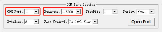
- Use the QCOM tool provided by Quectel to establish communication between the module and the PC via J0101 (USB interface). The following figure shows the field for setting the COM port on QCOM.Select the "COM port" (USB serial port) and set the correct "Baudrate". For more details about QCOM tool usage and configuration, see document [2].
Firmware Upgrade
You can use the JFlash tool provided by Quectel to establish the communication between the module and the PC via J0109 (SWD interface) or J0105 (JTAG interface).
NOTE:
Contact Quectel Technical Support for the JFlash tool. For more details about JFlash tool usage and configuration, see document [3].
Reset
To reset the module, first connect Module to KEY of J0114 (reset jumper interface), and then press and hold S0101 (reset button) for more than 100 ms before releasing it.
Appendix References
Related Documents:
| Document Name |
|---|
| [1]Quectel_HCM511S_Hardware_Design |
| [2]Quectel_QCOM_User_Guide |
| [3]Quectel_HCM511S_Test_Guide |
Terms and Abbreviations:
| Abbreviation | Description |
|---|---|
| COM | Communication |
| ETM | Embedded Trace Module (Macrocell) |
| GND | Ground |
| GPIO | General Purpose Input/Output |
| IC | Integrated Circuit |
| JTAG | Joint Test Action Group |
| LDO | Low-dropout Regulator |
| LED | Light Emitting Diode |
| PC | Personal Computer |
| RF | Radio Frequency |
| RXD | Receive Data (Pin) |
| SWD | Serial Wire Debug |
| SWO | Serial Wire Output |
| TXD | Transmit Data (Pin) |
| UART | Universal Asynchronous Receiver & Transmitter |
| USB | Universal Serial Bus |
| VBAT | Voltage at Battery (Pin) |